ORCAD Suite Using Layout
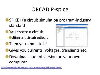
ORCAD Suite Using Layout. Drew Hall. Motivation. ORCAD is an entire software suite Schematic Simulation Layout ECO (Engineering Change Order) Seamless conversion between different components of software package Online DRC (Design Rule Checking) Industry standard software tool.

ORCAD Suite Using Layout
E N D
Presentation Transcript
ORCAD SuiteUsing Layout Drew Hall
Motivation • ORCAD is an entire software suite • Schematic • Simulation • Layout • ECO (Engineering Change Order) • Seamless conversion between different components of software package • Online DRC (Design Rule Checking) • Industry standard software tool
Schematics • Must use parts • Drawing boxes/lines/poly/… to create parts will NOT WORK!!! You must create parts! • Use off-page connectors, ports, hierarchal blocks, and busses to clean up schematics
Creating Parts 1. Create a new library (A library is a collection of parts) • File->New->Library 2. Create a new part • Right click on the library->Add New Part • Name the part, don’t change anything else 3. Draw the part outline using the Place Rectangle tool 4. Add pins using the Place Pin or the Place Pin Array tool
Migrating to Layout • Select the main design in the design window (the .dsn file) • Select Tools->Create Netlist • Select the Layout Tab • Check “Run ECO to Layout” • Select OK • Open ORCAD Layout • Select File->New
Migrating to Layout – Cont’d • Open the default technology (or a custom one) • Open the netlist created in ORCAD Capture • Select a filename to save the file as • Select footprints for parts • If a footprint does not already exist, choose ANY part that has the same number or more pins than your part. We will create the footprint later.
ORCAD Layout • Layout is based on a set of spreadsheets • Commonly used spreadsheets: • Layers – Contains information about all of the available layers on the board • Nets – Contains all of the nets imported from the netlist • Footprints – Contains all of the footprints in the design
Glossary • Footprint – Outline of a part and collection of pads • Pad – An area on the board for a pin to connect to • Padstack – A collection of pads for a part or project • Traces – Interconnection between different pads (nets) • Via (Blind, buried) – Via’s interconnect different layers • Ratsnest – All of the unrouted wires • CopperPour – Large area of copper material (can be used to make ground planes and many other things) • ThermalRelief – Copper pour on board to help with heat dissipation • DRC – Design Rule Check • Silkscreen (Nomenclature) – Text printed on board • Solder Mask – Chemical treatment on finished board to aid in manufacturability and ease assembly. Also protects board against minor abrasions and the environment • SMD – Surface Mount Devices (vs Through Hole Devices)
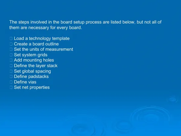
Board Outline • Select the Obstacle Tool • Right click and select new • Right click and select properties • Change the Obstacle Type to Board Outline • Change the Width to 12 • Change the Obstacle Layer to Global Layer • Select OK • Left click and draw board, double click when finished NOTE: • Boards can only have one board outline, make sure its on the global layer! • Some manufactures will not do fancy board outlines or cutouts in the middle of the board. Check with manufacturer or just keep it simple! • The pullback width is 1/2 the width of the board outline.
Creating Footprints • Start the Library Manager • Click on Create New Footprint • Name the footprint • Create the following obstacles: • Place Outline (Top Layer, width 6) • Detail Outline (SST Layer, width 6) • Detail Outline (AST Layer, width 6) • Open the padstacks spreadsheet • Create pads for the pins that you need • This is only required if the pads are not in the default technology file. Most pads are… this should only be necessary for special surface mount parts! • Select the Pin tool • Place all the pins • Edit the text on the SST and AST layers • Save! Do not forget to save. NOTE: • All of the information about the package is found in the datasheet, look it up! Don’t try and guess the size of the parts!!
Placing Components • Turn on reconnect mode (this hides the ratsnest and makes it easier to place the components) • Turn off the DRC • Select the component tool • Click on a component and move it to a new location (it must be inside of the board outline) • To rotate a part, press R while the part is selected • To place a part on the other side of the board, press 1 (for top layer) or 2 (for bottom layer) while the part is selected • Repeat step 4 until all components have been placed • Turn on the DRC • Turn off reconnect mode • Check for placement errors by clicking on Design Rule Check • To view errors, select the Errors spreadsheet • Fix all placement errors
Routing • Open the layers spreadsheet • Setup the layers by changing layer type between {Unused, Routing, and Plane} • Single sided board – Bottom (Routing), all others (Unused) • Double sided board – Top & Bottom (Routing), all outers (unused) • Multilayer board – Top, Bottom, inner layers (Routing or Plane), all others (unused) NOTE: • Plane layers can not be used for routing traces, if you want traces and a plane, then set the layer to routing rather than plane. A copper pour can be added later to simulate the plane.
Autorouting vs Manual • Autorouting • Traces are routed by the tool • Unfortunately, the autorouter that comes with the free version of ORCAD is not very good.. There are 3rd party tools that are VERY good, but also very expensive • Manual Routing • Time consuming • Ultimate control
Manual Routing • Select either the Edit Segment or the Add/Edit Route tool • The different tools work slightly differently, use which ever you are more comfortable with • Click on an unrouted net and route the net • To insert a via (connection between traces on different layers or traces and planes), press ‘V’ or click the mouse to end a segment and press the layer number (1 – top, 2 – bottom, 3 – ground, 4 – power, …) • If you have a plane layer, a connection is made to the plane layer by simply inserting a via (for through hole components, the connection is already made)
Autorouting • Select Auto->Autoroute->Board from the menu • Depending on the complexity of the board, this may take a very long time. • Do not think that this is the one step solution! You will need to go back and manual fix up the design. • Cleanup the design
Routing Tips • Always route power and ground traces first • Always route high frequency traces next • Avoid square corners, 45 and 135 are better • Avoid exiting pads at odd angles • Make traces sufficiently large for current capacity (http://www.geocities.com/CapeCanaveral/Lab/9643/TraceWidth.htm) • Minimize the number of vias • Avoid loops in ground traces, a plane or star configuration are the best
Mounting Holes • Select the component tool • Right click and create a new component • Name the component • Change the footprint to “MTHOLE1” • Place the component on the board • If you want to connect the hole to a net (say GND), use the connection tool to draw a net to ground • If you want smaller/larger mounting holes change the size of the footprint for MTHOLE1
Nomenclature • Select the text tool • Move around the text on the SST or SSB layers (do not worry about AST/ASB) • Right click and select new to add new text • Check with your manufacturer on the minimum line width. • Do not place nomenclature over vias, pads, or holes. It can go over traces but may not look quite as you expect it to.
Post Processing • Verify that there are no errors in the design (Auto->Design Rule Check) • Cleanup any errors before continuing • Run the post processor (Auto->Run Post Processor) • This will generate the Gerber files that the manufacturer will need to create the PCB. • Download a free Gerber view and check your files before you send them off.