Embedded Hardware
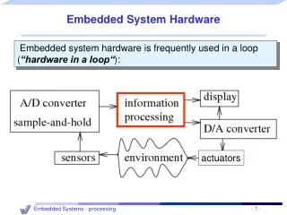
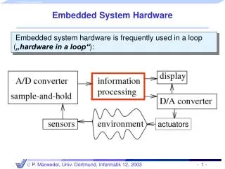
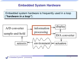
Embedded Hardware. Embedded System Hardware. Embedded system hardware is used for processing sensor input to produce output in task specific fashion. Information Processing System. Output Interface. Input Interface. Processors. Key requirements: Energy-efficiency


Embedded Hardware
E N D
Presentation Transcript
Embedded System Hardware • Embedded system hardware is used for processing sensor input to produce output in task specific fashion Information Processing System Output Interface Input Interface
Processors • Key requirements: Energy-efficiency High Code Density Microprocessors and Micro-controllers
CPU for Computers No RAM, ROM, I/O on CPU chip itself Example: Intel’s x86, Motorola’s 680x0 Microprocessors Many chips on mother-board Data Bus CPU General-Purpose Micro-processor Serial Port I/O Port RAM ROM Timer Address Bus General-Purpose Microprocessor System
What is Micro-controller? • Basically, a micro-controller is a device which integrates a number of the components of a microprocessor system onto a single microchip. • A micro-controller combines onto the same microchip: • The CPU core • Memory (both ROM and RAM) • Some parallel digital I/O
Micro-controller Source: www.ami.bolton.uk
Components of a Micro-controller • A Timer module to allow the micro-controller to perform tasks for certain time periods. • A serial I/O port to allow data to flow between the micro-controller and other devices such as a PC or another micro-controller. • An ADC to allow the micro-controller to accept analogue input data for processing.
Micro-controller Source : An Introduction to the design of small-scale embedded systems , Tim Wilmshurst, palgrave 2001
Why Micro-controller? • Low cost, small packaging • Low power consumption • Programmable, re-programmable • Lots of I/O capabilities • Easy integration with circuits • For applications in which cost, power and space are critical • Single-purpose
VonNeuman Architecture • Only one bus between CPU and memory • RAM and program memory share the same bus and the same memory, and so must have the same bit width • Bottleneck: Getting instructions interferes with accessing RAM Program and Data Memory CPU BUS
Data Memory CPU Program Memory 8-Bits 12/14/16-Bits Harvard Architecture • Separate program bus and data bus: can be different widths! • Instruction Pipelining easy
CISC – Complex Instruction Set Computer • A large number of instructions each carrying out a different permutation of the same operation • Instructions provide for complex operations • Different instructions of different format • Different instructions of different length • Different addressing modes • Requires multiple cycles for execution
RISC – Reduced Instruction Set Computer • Instructions for simple operations that can be executed in a single cycle • Each instruction of fixed length • Facilitates instruction pipelining • Large general purpose register set • Can contain data or address (symmetry) • Load-store Architecture • No memory access for data processing instructions
PIC Architecture PICs are “RISC” Reduced Instruction Set Computer (RISC) Few instructions (usually < 50) Only a few addressing modes Executes 1 instruction in 1 internal clock cycle (Tcyc)
The PIC Family: Packages PICs come in a huge variety of packages: Examples: 8 pin : 12C50x (12bit) and 12C67x (14bit) 18pin : 16C5X (12bit), 16Cxxx (14bit) 28pin : 16C5X (12bit), 16Cxxx (14bit) 40pin : 16Cxxx (14bit), 17C4x (16bit) 44 - 68pin : 16Cxxx (14bit), 17C4x / 17Cxxx (16bit)
PIC Mid-range Block Diagram Ref: PIC architecture reference manual
The PIC Family: Speed PICs require a clock to work. • Can use crystals, clock oscillators, or even an RC circuit. • Some PICs have a built in 4MHz RC clock • Not very accurate, but requires no external components! • Instruction speed = 1/4 clock speed (Tcyc = 4 * Tclk) • Examples 12C50x 4MHz 12C67x 10MHz 16Cxxx 20MHz 17C4x / 17C7xxx 33MHz 18Cxxx 40MHz
Clocking Scheme Ref: PIC architecture reference manual
Instruction Execution • Clock internally divided by 4 to generate 4 quadrature clocks • Instruction cycle consist of 4 Q cycles • PC incremented every Q1 • Instruction is fetched from program and latched into instruction register by Q4 • Instruction is decoded and executed in the following Q1 to Q4
Instruction Pipelining • Fetch takes one cycle, decode and execute takes another cycle • While execution, next instruction can be fetched • No bus conflict due to Harvard Architecture • If instruction changes PC ( e.g. Branch) extra cycle is required to complete instruction
Pipelining: Increasing Instruction Throughput Wash 1 2 3 4 5 6 7 8 1 2 3 4 5 6 7 8 Non-pipelined Pipelined Dry 1 2 3 4 5 6 7 8 1 2 3 4 5 6 7 8 non-pipelined dish cleaning Time pipelined dish cleaning Time Fetch-instr. 1 2 3 4 5 6 7 8 Decode 1 2 3 4 5 6 7 8 Fetch ops. 1 2 3 4 5 6 7 8 Pipelined Execute 1 2 3 4 5 6 7 8 Instruction 1 Store res. 1 2 3 4 5 6 7 8 Time pipelined instruction execution
Memory Organization • Program Memory • Register File Memory
The PIC Family: Program Memory PICs have two different types of program storage: 1. EPROM (Erasable Programmable Read Only Memory) • Note: One Time Programmable (OTP) chips are EPROM chips, but with no window! • PIC Examples: Any ‘C’ part: 12C50x, 17C7xx, etc. FLASH • Re-writable (even by chip itself) • Much faster to develop on! • Finite number of writes (~100k Writes) • PIC Examples: Any ‘F’ part: 16F84, 16F87x, 18Fxxx (future) • PIC program space is different for each chip.
Program Memory for your expt. • Used for storing compiled code • Each location is 14 bits long • Every instruction is coded as a 14 bit word • Addresses H’000’ and H’004’ are treated in a special way • PC can address up to (8K) addresses for (16F877)
The PIC Family: Data Memory PICs use general purpose “file registers” for RAM (each register is 8 bits for all PICs) • Don’t forget, programs are stored in program space (not in data space), so low RAM values are OK. • Register File Memory • Consist of 2 Components General Purpose Register (GPR) Files (RAM) Special Purpose Register (SPR) files • This portion of memory is separated into banks of 128 bytes long • 16F877 has 4 banks of register
Data Memory 4 banks • Important registers ─ STATUS ─ INDF ─ FSR ─ INTCON Use bit 5 and 6 of STATUS (RP0,RP1) to select bank # General purpose registers store user data Registers addressed directly, indirectly W register in accumulator
Register Addressing Modes • There are 3 types of addressing modes in PIC • Immediate Addressing • Direct Addressing • Indirect Addressing
Direct Addressing • Uses 7 bits of 14 bit instruction to identify a register file address • 8th and 9th bit comes from RP0 and RP1 bits of STATUS register.
Indirect Addressing • Full 8 bit register address is written the special function register FSR • INDF is used to get the content of the address pointed by FSR • Exp : A sample program to clear RAM locations H’20’– H’2F’ .
The PIC Family: Control Registers PICs use a series of “special function registers” for controlling peripherals and PIC behaviors. Some examples are: STATUS Bank select bits, ALU bits (zero, borrow, carry) INTCON Interrupt control: interrupt enables, flags, etc. TRIS Tristate control for digital I/O: which pins are ‘floating’ TXREG UART transmit register: the next byte to transmit
Status Register • Status bits ─ Bit 0: Carry ─Bit 1: Digit carry ─ Bit 2: Zero result ─ Bits 3 & 4: Use at power-up and sleep ─ Bit 5 & 6: bank select ─Bit 7: bank select for indirect addressing
The PIC Family: Peripherals Different PICs have different on-board peripherals Some common peripherals are: • Tri-state (“floatable”) digital I/O pins • Analog to Digital Converters (ADC) • Serial communications: UART (RS-232C), SPI, I2C, CAN • Pulse Width Modulation (PWM) • Timers and counters • Watchdog timers
PIC Peripherals: Digital I/O) • All PICs have digital I/O pins, called ‘Ports’ • the 8pin 12C508 has 1 Port with 4 digital I/O pins • the 68pin 17C766 has 9 Ports with 66 digital I/O pins • Ports have 2 control registers • TRISX sets whether each pin is an input or output • PORTX sets their output bit levels • Most pins have 25mA source/sink (directly drives LEDs)
PIC Peripherals: ADCs • Only available in 14 bit and 16 bit cores • Most 8 bits, newer PICs have 10 or 12 bits • Theoretically higher accuracy when PIC is in sleep mode (less digital noise) • Can generate an interrupt on ADC conversion done • Must wait Tacq to charge up sampling capacitor (see datasheets)
PIC Peripherals: Timers • Available in all PICs. • 14+ bit cores may generate interrupts on timer overflow. • Some 8 bits, some 16 bits, some have prescalers • Can use external pins as clock in/clock out(ie, for counting events or using a different Fosc) • Warning: some peripherals share Timer resources
PIC Timers • The device has three readable and writeable hardware timers that can increment automatically each instruction cycle (if no prescaler is used). All timers can cause an interrupt on overflow, and then restart from zero
PIC Timers / Timer 0 • 8 bit timer/counter with prescaler • Readable and writeable • 8-bit software programmable prescaler • Internal or external clock set • Interrupt on overflow from 0xFF to 0x00 • Edge Select for external clock
PIC Timers / Timer 1 • 16-bit timer/counter with prescaler • Readable and writeable • 1, 2, 4, 8 programmable prescaler • Internal or external clock select • External clock can be syn. or asyn. • Interrupt on overflow • Second crystal permitted
PIC Timers / Timer 2 • 8-bit timer/counter with prescaler and postscaler • Readable and writeable • 1,4 or 16 programmable prescaler • 4-bit programmable postscaler • Interrupt on overflow • Output to port pin
Timers • TIMER0 is an 8-bit timer with an eight bit prescaler, which can make the timer run 2 to 256 times slower than normal • TIMER1 is a 16-bit timer (two 8-bit registers) with a 1:1 to 1:8 prescaler and some other features. Used by given C code to generate soft timer and sound • TIMER2 is an 8-bit timer with 1:1 to 1:16 prescaler and a 1:1 to 1:16 postscaler It also has a period register.Used by given C code for PWM motor control • Watch Dog Timer
PIC Peripherals: CCP Modules • Capture/Compare/PWM (CCP) • 10 bit PWM width within 8bit PWM period(frequency) • Enhanced 16bit cores have better bit widths • Frequency/Duty cycle resolution tradeoff • 19.5KHz has 10bit resolution • 40KHz has 8bit resolution • 1MHz has 1bit resolution (makes a 1MHz clock!) • Can use PWM to do DAC - See AN655 • Capture counts external pin changes • Compare will interrupt on when the timer equals the value in a compare register
PIC Peripherals: Misc. • Sleep Mode: PIC shuts down until external interrupt (or internal timer) wakes it up. • Interrupt on pin change: Generate an interrupt when a digital input pin changes state (for example, interrupt on keypress). • Watchdog timer: Resets chip if not cleared before overflow • Brown out detect: Resets chip at a known voltage level • LCD drivers: Drives simple LCD displays • VIRTUAL PERIPHERALS: • Peripherals programmed in software. USART, timers, and more can be done in software (but it takes most of the resources of the machine)
Low End: 12C508 • 8pin package (DIP, SO) • 12bit core - 33 instructions • 1us instruction time (Tclk = 4MHz) • 512 12bit program memory • 25 8bit data memory or registers (“File registers”) • 2 level hardware stack (no interrupts) • 5 GPIO pins, 1 input only (25mA source/sink) • Features: wake up on pin change, internal oscillator • Peripherals: Timer, Watch Dog Timer
Mid Range: 16F876 • 28pin package (DIP, SO) • 14bit core - 35 instructions • 200ns instruction time (Tclk = 20MHz) • 8,092 14bit FLASHprogram memory • 368 8bit data memory or registers (“File registers”) • 256 8bit EEPROM (nonvolatile) data registers • 8 level hardware stack (interrupts enabled) • 22 GPIO (20mA source / 25mA 7sink) • Peripherals: 5ch 10bit ADC, USART/I2C/SPI, 16bit & 8bit timers • Features: Brown out detect, In-Circuit Debugger (ICD)
High End: 17C766 • 84pin PLCC package • 16bit core - 58 instructions • 121ns instruction time (Tclk = 33MHz) • 16,384 16bit program memory • 902 8bit data memory or registers • 16 level hardware stack (priority interrupts) • 66 GPIO (20mA source / 35mA sink) • Peripherals: • 2x 16bit + 2x 8bit timer, WDT, 2x USART, 4x CCP, • 12ch 10bit ADC