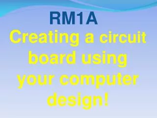
Creating Circuit Boards with Computer-Aided Design
Learn how to design and fabricate circuit boards using your computer. Understand schematic diagrams, symbols for electronic parts, and software for circuit design. Follow steps for transferring designs onto copper-clad boards and etching circuits safely. Tips for cleaning boards, bonding film, and etching with acid solution provided. Includes instructions for touch-ups and safety precautions. Get hands-on experience creating circuit boards for your projects.

Creating Circuit Boards with Computer-Aided Design
E N D
Presentation Transcript
RM1A Creating a circuit board using your computer design!
Most student developed circuit boards come from Schematic Diagrams that are found in books or online. The Schematic diagram such as the one shown below, is a map showing what parts connect to one another, as well as HOW they connect.
In order to be able to identify the parts that are shown in a schematic diagram, the student must know the symbols which are used that represent the physical electronic parts. Below, on the left side, you will see a few of the schematic symbols which are used in drawing schematic diagrams. On the right side you will see the physical electronic parts that the symbol represents. Schematic symbols Physical electronic parts LED’S TRANSISTOR’S
There are many software programs that allow the user to design and layout a circuit board on a computer. For basic circuits, any art program will do as long as you can make lines and circles. The student would use a schematic diagram as a guide to develop a circuit board layout. Below on the left you see a basic schematic circuit. On the right, a basic circuit board layout has been created so that the parts can be interconnected on a piece of copper clad board.
Since the robot control boards are complex circuits, the design has been completed for you. Your teacher will help you print the circuit board design for your robot control board on blue film “release” paper and help you get the circuit “ironed-on” to the copper clad circuit board for etching!
In order to get the blue film to adhere to the copper board properly, the copper clad board must be cleaned to remove any unwanted oxidation. Your teacher may hand you a copper board and a scrub pad or fine grit sandpaper to clean your board before placing the film and board in the heat press for bonding.
Oxidized copper board that needs to be cleaned. 400 grit sandpaper may also be used to remove the oxidation from the board. Scotch brite “scrub” pad for cleaning the board.
You can scrub the board in a sink area and it helps if you use some water when you scrub the board.
400 grit wet-dry sandpaper may also be used to clean the board. Water is necessary as a lubricant when removing the oxidation from the board.
When you have cleaned the board and dried it properly, it should look shiny with no fingerprints or dark areas. Your instructor can inspect your board to be sure it is ready for film. The scratchy looking areas are from the abrasive that was used to clean the board and will cause no problems in the transfer process.
The film can now be placed shiny side up on the copper clad board and the two parts can be placed into the heat press at 350 degrees for 45 seconds. Be sure to use something other than your hand to remove the board from the press because it will be HOT!
After cooling for about 3 minutes, the board must go back into the press for a 2nd time for 45 seconds. This is to ensure a good bond between the diagram and the copper. After it is removed from the heat press for the second time, the circuit design should have a slightly embossed look to the line traces. You will need to hold board under a light source to see the detail.
If the circuit is still not bonded well enough, a third heat set might be required for no more than 20 seconds.
Once the board has cooled slightly, carefully peel back the film (slowly) to see the finished transfer.
Any areas which DID NOT transfer well, may be touched up using a black permanent marker. Be sure to only color in the areas of blue that are missing and DO NOT cover up or connect any traces that should NOT connect. The permanent marker PREVENTS acid from eating away the “Good” copper!
This picture shows where the marker was used to touch up a blue film transfer on a robot control board.
Below you will see what a basic etching tank looks like. The air pump is used to circulate the water as the copper gets eaten away by the acid. The etchant is a combination of Muriatic Acid and Peroxide. At the end of this slideshow, in the APPENDIX, you will find a handout that tells how to mix the etchant. To etch a board, you simply place the board into the tank. YOU SHOULD ALWAYS USE RUBBER GLOVES AND WEAR SAFETY GLASSES. Try NOT to get your hands in contact with the acid. If contact occurs, wash your hands immediately.