
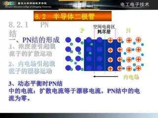
8.2.1 PN 结
8.2.1 PN 结. 8.2 半导体二极管. 空间电荷区. N. P. 耗尽层. 一、 PN 结的形成. 1 、浓度差引起载流子的扩散运动. 2 、内电场引起载流子的漂移运动. 内电场. 3 、动态平衡时 PN 结 中的电流:扩散电流等于漂移电流, PN 结中的电流为零。. 空间电荷区变窄. I. 外电场方向. E. 二、 PN 结的单向导电特性. 外电场驱使 P 区的空穴进入空间 电荷区抵消一部分负空间电荷. N 区电子进入空间电荷区 抵消一部分正空间电荷. P 区. N 区. 内电场方向. R. 扩散运动增强,形

8.2.1 PN 结
E N D
Presentation Transcript
8.2.1 PN 结 8.2 半导体二极管 空间电荷区 N P 耗尽层 一、PN结的形成 1、浓度差引起载流子的扩散运动 2、内电场引起载流子的漂移运动 内电场 3、动态平衡时PN结 中的电流:扩散电流等于漂移电流,PN结中的电流为零。
空间电荷区变窄 I 外电场方向 E 二、PN结的单向导电特性 外电场驱使P区的空穴进入空间 电荷区抵消一部分负空间电荷 N区电子进入空间电荷区 抵消一部分正空间电荷 P 区 N 区 内电场方向 R 扩散运动增强,形 成较大的正向电流 (1)外加正向电压
空间电荷区变宽 IR 外电场方向 E 外电场驱使空间电荷区两侧的空穴和自由电子移走 多数载流子的扩散运动难于进行 P 区 N 区 少数载流子越过 PN 结形成很小的反向电流 内电场方向 R (2)外加反向电压
三、PN结的击穿 1、齐纳击穿:(击穿电压低)4伏以下。 浓度高时,PN结窄,在同样电压下,反向电场很强,从而破坏共价键的结构,把电子拉出来。 2、雪崩击穿:(击穿电压高)6伏以上。 浓度低时,:PN结宽,电子在PN结中被加速,当遇到价电子时,就可以把其撞出来。 3、4伏~6伏,两种情况都可能电击穿