FM Transmitter
FM Transmitter. FM Modulation using VCO. [1]. f out. V in. - Free Running Frequency of VCO. Corresponding DC bias. - Gain of VCO. Block Diagram. PA. . VCO. Input. DC Bias Vcc/2. Chipset. 4046 Phase-Locked Loop LM7171 Wide-Band Power Amplifier 741 Op Amp. 4046 PLL .

FM Transmitter
E N D
Presentation Transcript
FM Modulation using VCO [1] fout Vin - Free Running Frequency of VCO Corresponding DC bias - Gain of VCO
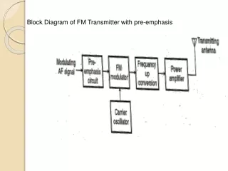
Block Diagram PA VCO Input DC Bias Vcc/2
Chipset • 4046 Phase-Locked Loop • LM7171 Wide-Band Power Amplifier • 741 Op Amp
4046 PLL Only use the VCO
4046 VCO Characteristic C1>=100pF
PCB Layout Considerations • The signal traces should be short and wide to lower the impedance. • The width of the signal traces has to satisfy current driving capacity. • Any used board area should be shorted to ground to reduce AC noise. • Sockets and pads will induce extra capacitance, so components should be directly soldered to board. • Surface mount components are preferred over discrete ones for less lead inductance.
Measured Results • Carrier Frequency: 15MHz • Bandwidth: Controllable • Output Power: 500mW
FM Demodulation using PLL [2] PFD LF Ve in VCO
VCO Design • VCO free running frequency = Carrier Frequency • VCO Frequency Range is no smaller than Bandwidth • Large VCO gain will increase PLL natural frequency n and thus improves PLL tracking capability
Block Diagram LNA Amp BPF PFD LF VCO
Chipset • 4046 PLL • CLC425 Wide-band LNA
Block Diagram IF Amp + IF Filter Input Matching Mixer Amp FM Demodulator LO
Chipset • TDA7000 – FM Radio • LM3875 – Audio Power Amplifier
TDA7000 [4]
Quadrature Demodulator Vout fin
IF Harmonic Distortion IF=70kHz
Correlator To suppress interstation noise • Not Modulated • Lightly Modulated • Heavily Modulated
PLL Reference Frequency Output Dual Modulus Prescaler Digital Input A/D Converter Shift Register Analog Input Clock Data Sampling Rate Block Diagram
Output Driver To drive capacitive load with minimum delay
Capacitor Driving Capability CL=100p f=50MHz