The Rise of ASICs: Meeting the Demand for High-Performance Integration
This lecture series explores the role of Application-Specific Integrated Circuits (ASICs) in modern technology. With increasing demands for higher performance and optimization in various applications from smartphones to supercomputers, ASICs provide tailored solutions. The series covers essential topics such as CMOS technology advancements, the implications of Moore's Law, and the challenges of designing complexity into billion transistor chips. Discussions also target design costs and efficiency, providing insights into the future of integrated circuit design and development.

The Rise of ASICs: Meeting the Demand for High-Performance Integration
E N D
Presentation Transcript
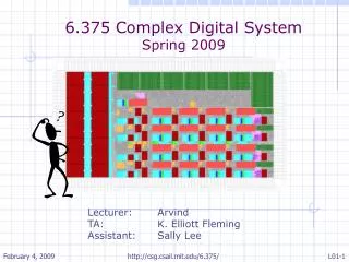
6.375 Complex Digital System Spring 2007 Lecturers: Arvind & Krste Asanović TAs: Myron King & Ajay Joshi Assistant: Sally Lee http://csg.csail.mit.edu/6.375/
Do we need more chips (ASICs)?ASIC=Application-Specific Integrated Circuit http://csg.csail.mit.edu/6.375/
Wide Variety of Products Rely on ASICs Sensor Nets Cameras Games Set-top boxes Media Players Laptops Servers Robots Smart phones Routers Automobiles Supercomputers http://csg.csail.mit.edu/6.375/
Source: http://www.intel.com/technology/silicon/mooreslaw/index.htm What’s required? ICs with dramatically higher performance, optimized for applications and at a • size and power to deliver mobility • cost to address mass consumer markets http://csg.csail.mit.edu/6.375/
Let’s take a look at current CMOS technology... http://csg.csail.mit.edu/6.375/
“Glass” on top seals chip “Vias” connect one layer to another Thicker wires on higher layers used for power and ground, and long range signals Wiring added in layers on top of wafer Thinner wires on lower layers used for dense local wiring Transistors fabricated first on original surface of wafer Bulk of wafer Chip = Transistors + Wires Cross-section through IBM 90nm process, 10 metal layers [ISSCC 2004] http://csg.csail.mit.edu/6.375/
gate inversionhappens here Surface of wafer Source diffusion Drain diffusion Ev Eh bulk Reverse side of wafer FET = Field-Effect TransistorA four terminal device (gate, source, drain, bulk) Inversion: A vertical field creates a channel between the source and drain. Conduction: If a channel exists, a horizontal field causes a drift current from the drain to the source. http://csg.csail.mit.edu/6.375/
Simplified FET Model Binary logic values represented by voltages: “High” = Supply Voltage, “Low” = Ground Voltage Supply Voltage = VDD S PFET connects S and D when G=“low”=0V G PFET only good at pulling up G D D NFET connects D and S when G=“high”=VDD NFET only good at pulling down G G S Ground = GND = 0V http://csg.csail.mit.edu/6.375/
NAND Gate (A.B) (A.B) A B B A • When both A and B are high, output is low • When either A or B is low, output is high http://csg.csail.mit.edu/6.375/
Parallel PMOS Transistors VDD P-Diffusion (in N-well) (A.B) (A.B) B A Poly wire connects PMOS & NMOS gates Output on Metal-1 Metal 1-Diffusion Contact A B GND N-Diffusion Series NMOS Transistors NAND Gate Layout http://csg.csail.mit.edu/6.375/
Exponential growth: Moore’s Law Intel 8086, 1978, 33mm2 10Mhz, 29K transistors, 3u Intel 80286, 1982, 47mm2 12.5Mhz, 134K transistors, 1.5u Intel 386DX, 1985, 43mm2 33Mhz, 275K transistors, 1u Intel 8080A, 19743Mhz, 6K transistors, 6u Intel 486, 1989, 81mm2 50Mhz, 1.2M transistors, .8u Intel Pentium, 1993/1994/1996, 295/147/90mm2 66Mhz, 3.1M transistors, .8u/.6u/.35u Intel Pentium II, 1997, 203mm2/104mm2 300/333Mhz, 7.5M transistors, .35u/.25u Shown with approximate relative sizes http://www.intel.com/intel/intelis/museum/exhibit/hist_micro/hof/hof_main.htm http://csg.csail.mit.edu/6.375/
Intel Penryn (2007) • Dual core • Quad-issue out-of-order superscalar processors • 6MB shared L2 cache • 45nm technology • Metal gate transistors • High-K gate dielectric • 410 Million transistors • 3+? GHz clock frequency Could fit over 500 486 processors on same size die. http://csg.csail.mit.edu/6.375/
.. But Design Effort Growing Nvidia Graphics Processing Units Transistors (M) 9x growth in back-end staff • Front-end is designing the logic (RTL) • Back-end is fitting all the gates and wires on the chip; meeting timing specifications; wiring up power, ground, and clock Relative staffing on back-end Design Effort per Chip 5x growth in front-end staff Relative staffing on front-end http://csg.csail.mit.edu/6.375/
Design Cost Impacts Chip Cost • 90nm ASIC cost breakdown, $30M total (Altera study): • 59% chip design (architecture, logic & I/O design, product & test engineering) • 30% software and applications development • 11% prototyping (masks, wafers, boards) • If we sell 100,000 units, Non-Recurring Engineering (NRE) costs add $30M/100K = $300 per chip! • Example above is for design using automated tools • Similar to what we’ll be using in 6.375 • Hand-crafted IBM-Sony-Toshiba Cell microprocessor achieves 4GHz in 90nm, but development cost was >$400M http://csg.csail.mit.edu/6.375/
Topics to address in 6.375 • How can we design complex billion transistor ASICs with reasonable effort? • How good are our designs? • Performance, area, power http://csg.csail.mit.edu/6.375/
LPM Pipeline example: • Which is best? Designer’s Dilemma ASIC Complexity • 2000: 1M+ logic gates • 2005: 10M+ logic gates • 2010: 100M+ logic gates Constants • 10-30 person design team size • 18 month design schedule • Design flow -- unchanged for 10+ years! Designer must take shortcuts • Conservative design • No time for exploration • Educated guess & code • Gates are free mentality [ICCAD’04] What happens when a designer must implement a 1M gate block? Sub-optimal implementations! Alternatives? http://csg.csail.mit.edu/6.375/
6.375 Course Philosophy • Effective abstractions to reduce design effort • High-level design language rather than logic gates • Control specified with Guarded Atomic Actions rather than with finite state machines • Guarded module interfaces automatically ensure correctness of composition of existing modules • Design discipline to avoid bad design points • Decoupled units rather than tightly coupled state machines • Design space exploration to find good designs • Architecture choice has largest impact on solution quality A unified view of languages, disciplines and tools that supports rapid design space exploration to find best area, power, and performance point with reduced design effort http://csg.csail.mit.edu/6.375/
6.375 ObjectivesBy end of term, you should be able to: • Decompose system requirements into a hierarchy of sub-units that are easy to specify, implement, and verify, and which can be reused • Develop efficient verification and test plans • Select appropriate microarchitectures for a unit and perform microarchitectural exploration to meet price, performance, and power goals • Use industry-standard tool flows • Complete a working million gate chip design! • Make millions $$$ at a new chip startup (Don’t forget your alma mater!) http://csg.csail.mit.edu/6.375/
6.375 Prerequisites • You must be familiar with undergraduate (6.004) logic design : • Combinational and sequential logic design • Dynamic Discipline (clocking, setup and hold) • Finite State Machine design • Binary arithmetic and other encodings • Simple pipelining • ROMs/RAMs/register files • Additional circuit knowledge (6.002, 6.374) useful but not vital • Architecture knowledge (6.823) helpful for projects http://csg.csail.mit.edu/6.375/
6.375 Structure • First half of term (before Spring Break) • Lecture or tutorial MWF, 2:30pm to 4:00pm in 32-124 • Three labs (on Athena, lab machines in 38-301) • Form project teams (2-3 students); prepare project proposal (watch website for project ideas) • Closed-book 90 minute quiz (Friday before Spring Break) • Second half of term (after Spring Break) • Weekly project milestones, with 1-2 page report • Weekly project meeting with the instructors and TAs • Final project presentations in last week of classes • Final project report (~15-20 pages) due Thursday May 17 (no extensions) http://csg.csail.mit.edu/6.375/
6.375 Grade Breakdown • Three labs 30% • Quiz 20% • Five project milestones 25% • Final project report 25% (including presentation) http://csg.csail.mit.edu/6.375/
6.375 Collaboration Policy • We strongly encourage students to collaborate on understanding the course material, BUT: • Each student must turn in individual solutions to labs • Students must not discuss quiz contents with students who have not yet taken the quiz • If you’re inadvertently exposed to quiz contents before the exam, by whatever means, you must immediately inform the instructors or TA http://csg.csail.mit.edu/6.375/
ASIC Design Styles http://csg.csail.mit.edu/6.375/
Hardware Design Abstraction Levels Application Algorithm Unit-Transaction Level (UTL) Model Guarded Atomic Actions (Bluespec) Register-Transfer Level (Verilog RTL) Gates Circuits Devices Physics http://csg.csail.mit.edu/6.375/
ASIC Design Styles • Full-Custom (every transistor hand-drawn) • Best possible performance: as used by Intel mPs • Semi-Custom (Some custom + some cell-based design) • Reduced design effort: AMD mPs plus recent Intel mPs • Cell-Based ASICs (Only use cells in standard library) • High-volume, moderate performance: Graphics chips, network chips, cellphone chips • This is what we’ll use in 6.375 • Mask-Programmed Gate Arrays/Structured ASICs • Medium-volume, moderate performance applications • Field-Programmable Gate Arrays • Low-volume, low-moderate performance applications, and prototyping • Comparing styles: • how many design-specific mask layers per ASIC? • how much freedom to develop own circuits? • what design methods and tools are needed? http://csg.csail.mit.edu/6.375/
Custom and Semi-Custom • Usually, in-house design team develops own libraries of cells for commonly used components: • memories • register files • datapath cells • random logic cells • repeaters • clock buffers • I/O pads • In extreme cases, every transistor instance can be individually sized ($$$$) • approach used in Alpha microprocessor development • The trend is towards greater use of semi-custom design style • use a few great circuit designers to create cells • redirect most effort at microarchitecture and cell placement to keep wires short http://csg.csail.mit.edu/6.375/
Custom Designer works with Low-Level Design Rules Extension rules Exclusion rule Surround rule • An abstraction of the fabrication process that specify various geometric constraints on how different masks can be drawn • Design rules can be absolute measurements (e.g. in nm) or scaled to an abstract unit, the lambda. The value of lambda depends on the manufacturing process finally used. Width rules Spacing rules http://csg.csail.mit.edu/6.375/
Mem 1 Mem 2 Standard Cell ASICsaka Cell-Based ICs (CBICs) • Fixed library of cells + memory generators, often provided by fabrication foundry or third-party library providers • Cells can be synthesized from HDL, or entered in schematics • Cells placed and routed automatically • Requires complete set of custom masks for each design • Currently most popular hard-wired ASIC type (6.375 will use this) Cells arranged in rows Generated memory arrays http://csg.csail.mit.edu/6.375/
Standard Cell Library Components Well Contact under Power Rail Clock Rail (not typical) • Cells have standard height but vary in width • Designed to connect power, ground, and wells by abutment Clock Rail VDD Rail Cell I/O on M2 Power Rails in M1 GND Rail NAND2 Flip-flop http://csg.csail.mit.edu/6.375/
Blueview C CycleAccurate Bluespec C sim RTL synthesis gates Legend files Bluespec tools 3rd party tools 6.375 Standard Cell Design Flow Bluespec SystemVerilog source Bluespec Compiler Verilog 95 RTL Verilog sim VCD output Debussy Visualization Place & Route Physical Tapeout http://csg.csail.mit.edu/6.375/
Standard Cell Design Examples Channel routing for 1.0mm 2-metal stdcells Over cell routing for 0.18mm 6-metal stdcells http://csg.csail.mit.edu/6.375/
GND NMOS PMOS VDD PMOS NMOS GND [ OCEAN Sea-of-Gates Base Pattern ] Mask-Programmed Gate Arrays • Can cut mask costs by prefabricating arrays of fixed size transistors on wafers • Only customize metal layer for each design Two kinds: • Channeled Gate Arrays • Leave space between rows of transistors for routing • Sea-of-Gates • Route over the top of unused transistors http://csg.csail.mit.edu/6.375/
Gate Array Personalization Isolating transistors by shared GND contact Isolating transistors with “off” gate GND http://csg.csail.mit.edu/6.375/
Gate Array Pros and Cons • Cheaper and quicker since less masks to make • Can stockpile wafers with diffusion and poly finished • Memory inefficient when made from gate array • Embedded gate arrays add multiple fixed memory blocks to improve density (=>Structured ASICs) • Cell-based array designed to provide efficient memory cell (6 transistors in basic cell) • Logic slow and big due to fixed transistors and wiring overhead • Advanced cell-based arrays hardwire logic functions (NANDs/NORs/LUTs) which are personalized with metal http://csg.csail.mit.edu/6.375/
Field-Programmable Gate Arrays (FPGAs) • Arrays mass-produced and programmed by customer after fabrication • Can be programmed by blowing fuses, loading SRAM bits, or loading FLASH memory • Each cell in array contains a programmable logic function • Array has programmable interconnect between logic functions • Overhead of programmability makes arrays expensive and slow but startup costs are low, so much cheaper than ASIC for small volumes http://csg.csail.mit.edu/6.375/
Xilinx Configurable Logic Block http://csg.csail.mit.edu/6.375/
FPGA Pros and Cons Advantages • Dramatically reduce the cost of errors • Remove the reticle costs from each design Disadvantages (as compared to an ASIC) [Kuon & Rose, FPGA2006] • Switching power around ~12X worse • Performance up 3-4X worse • Area 20-40X greater Still requires tremendous design effort at RTL level http://csg.csail.mit.edu/6.375/