Dual-port Memory WRITE
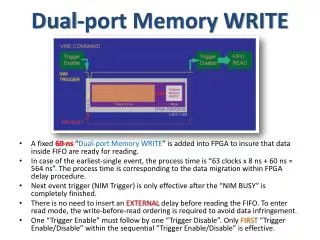
Dual-port Memory WRITE. A fixed 60-ns “ Dual-port Memory WRITE ” is added into FPGA to insure that data inside FIFO are ready for reading.

Dual-port Memory WRITE
E N D
Presentation Transcript
Dual-port Memory WRITE • A fixed 60-ns “Dual-port Memory WRITE” is added into FPGA to insure that data inside FIFO are ready for reading. • In case of the earliest-single event, the process time is “63 clocks x 8 ns + 60 ns = 564 ns”. The process time is corresponding to the data migration within FPGA delay procedure. • Next event trigger (NIM Trigger) is only effective after the “NIM BUSY” is completely finished. • There is no need to insert an EXTERNALdelay before reading the FIFO. To enter read mode, the write-before-read ordering is required to avoid data infringement. • One “Trigger Enable” must follow by one “Trigger Disable”. Only FIRST“Trigger Enable/Disable” within the sequential “Trigger Enable/Disable” is effective.
Latch Card Testing by CODA NIM FAN-IN/FAN-OUT NIM Delay Box Delay Box = 128 ns Delay Box = 0 ns W/O Delay Box VME LATCH CARD • Data taken through CODA • GrassTest_572.dat • GrassTest_573.dat • GrassTest_574.dat TRIGGER VME SIS3610 NIM NIM-ECL/ECL-NIM