Download
1 / 26
260 likes | 412 Vues
This document provides a comprehensive overview of the 68HC12 Analog-to-Digital (ATD) Converter System. It covers fundamental concepts of analog-to-digital conversion, including transducer interface design, conversion processes, sampling rates, encoding, quantizing, resolution, and data rates. Detailed explanations of the ATD registers, including control, status, result, and test registers, are provided. Key programming concepts for the ATD system are also discussed, aiming to equip readers with the necessary knowledge to design and implement effective analog-to-digital conversion solutions.

E N D
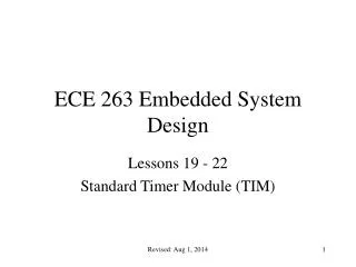
ECE 263 Embedded System Design Lessons 16 - 18 68HC12 Analog-to-Digital (ATD) Converter System Revised: Aug 1, 2014
Overview • Analog-to-digital fundamental concepts • 68HC12 ATD system description • ATD registers • control registers • status registers • result registers • test registers • ATD programming Revised: Aug 1, 2014
Analog-to-digital fundamental concepts • Transducer interface design • Big picture • conversion process • sampling rate • encoding • quantizing and resolution • data rate • successive approximation converter Revised: Aug 1, 2014
Analog-to-digital fundamental conceptsTransducer Interface Design • We live in an analog world! • Physical variable requires conversion to digital representation • i.e. light, pressure, temperature -> voltage -> binary • Requires transducer for conversion • Transducer requires interface to microprocessor such that it fills conversion window (VRH - VRL) Revised: Aug 1, 2014
Analog-to-digital fundamental conceptsTransducer Interface Design (cont) V2max = V2min * K + B V1max = V1min * K + B Revised: Aug 1, 2014
Analog-to-digital fundamental conceptsBig Picture Revised: Aug 1, 2014
Analog-to-digital fundamental conceptsconversion process • conversion process • sampling rate • encoding • quantizing and resolution • data rate Revised: Aug 1, 2014
Analog-to-digital fundamental conceptsconversion process - sampling rate • strobe light example • Nyquist criterion: sample signal at a minimum frequency of twice the highest frequency content of the sampled signal fs >= 2 fh • Time interval between samples Ts = 1/ fs • anti-aliasing filter: use LPF with fcutoff = fh • phone company samples human voice at 8 KHz, uses 4 KHz LPF to prevent aliasing Revised: Aug 1, 2014
Analog-to-digital fundamental conceptsconversion process - encoding • Provides unique binary code for every discrete voltage step between VRH and VRL n = 2b 4.375V 3.750V 3.125V 2.500V 1.875V 1.250V 0.625V Revised: Aug 1, 2014
Analog-to-digital fundamental conceptsconversion process - quantizing, resolution, data rate • Quantization: number of discrete levels the analog signal is divided into between VRH and VRL • More levels provide better representation of sampled signal EX] VRH = 5 VDC and VRL = 0 VDC, quantization 256 levels voltage per step = (5V - 0V)/(256 steps) = 19.53 mV/step • Resolution: voltage per step Resolution = (VRH - VRL)/number of steps = (VRH - VRL)/2b • Data rate: d = fsb Revised: Aug 1, 2014
Analog-to-digital fundamental conceptsconversion process - successive approximation Revised: Aug 1, 2014
68HC12 ATD system description Revised: Aug 1, 2014
68HC12 ATD system description (cont) • Eight ATD analog inputs on PORTAD PAD[7:0] • Inputs fed to analog multiplexer • Single signal fed to successive approximation converter • Initiate conversion by writing to control register • Upon conversion complete appropriate flags set in status registers • Results available in results register Revised: Aug 1, 2014
ATD registers • control registers - configures ATD for specific operation (ATDCTL0 - ATDCTL5) • status registers - two-byte register containing ATD status flags (ATDSTAT) • result registers - contains binary weighted result after conversion (ADR0H - ADR7H) • test registers - used in special modes Revised: Aug 1, 2014
ATD registerscontrol registers • Used to tailor an ATD conversion sequence • We will concentrate on control registers ATDCTL 2, 4, and 5 Revised: Aug 1, 2014
ATD registerscontrol registers - ATDCTL2 • Memory address: $0062 • ADPU: “on/off” switch • 0: off, 1: on (0 after processor reset) • must wait 100 us after “on” prior to using ATD • AFFC: ATD Fast Flag Clear • 0: normal clearing - write to ATDCTL5 • 1: fast clearing - cleared when first result register read Revised: Aug 1, 2014
ATD registerscontrol registers - ATDCTL4 • Memory address: $0064 • Controls sample timing for conversion sequence Revised: Aug 1, 2014
ATD registerscontrol registers - ATDCTL5 • Used to configure conversion mode for ATD • Memory location: $0065 • S8CM: select 8 channel mode 0: four, 1: eight conversions • SCAN: enable continuous scan 0: single 1: continuous conversion • MULT: enable multiple channel conversion 0: single channels, 1: multiple channels • CD,CC,CB,CA: specify channels for conversion Revised: Aug 1, 2014
ATD registerscontrol registers - ATDCTL5 (cont) Revised: Aug 1, 2014
ATD registersstatus registers • two-byte register containing ATD status flags (ATDSTAT) • contains series of flags that indicate status of the ATD • Sequence Complete Flag (SCF) indicates specified conversion is complete • CCx: 3 bit counter which indicates channel currently undergoing conversion • CCFx: Conversion Complete Flag for each result register Revised: Aug 1, 2014
ATD registersresult registers • After conversion results placed in ADR0H-7H • Unsigned, weighted binary result 1/2FS 1/4FS 1/8FS…. • VDC = (contents ADRxH/256) * (VRH - VRL) Revised: Aug 1, 2014
ATD Programming Revised: Aug 1, 2014
ATD Programming Revised: Aug 1, 2014
ATD Programming Revised: Aug 1, 2014
ATD Programming Revised: Aug 1, 2014
ATD Programming Revised: Aug 1, 2014