Download
1 / 1
10 likes | 110 Vues
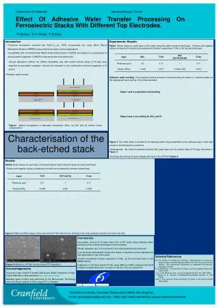
Study on the effect of adhesive wafer transfer processing on ferroelectric stacks with different top electrodes. Techniques involve dry etching Si, SiO2, and Pt layers. Successful removal of Pt base layer shown.

E N D
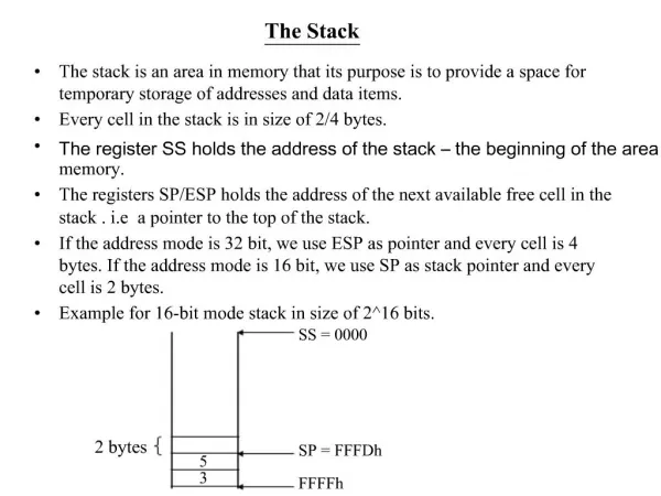
Figure 6 Hillocks in a Pt film formed during PZT deposition Department of Materials Nanotechnology Centre Effect Of Adhesive Wafer Transfer Processing On Ferroelectric Stacks With Different Top Electrodes. 1P.Gkotsis, 1R.V. Wright, 1P.B.Kirby • Experiments- Results • Table1 Stress values for each layer of the stack using the wafer curvature technique. Positive and negative values correspond to tensile and compressive stresses respectively. Ti-Au is the top electrode layer. • Adhesive wafer bonding. The template removal process involves bonding the stack on a backing wafer for the subsequent back etching of the initial substrate. • Figure 2 The initial wafer is bonded to the backing wafer using polyamide as the adhesive layer under high pressure and temperature conditions • Subsequently the initial Si substrate and the SiO2 base layer are dry etched. Back of Pt layer illustrated in Figure 3 • Final step dry etching Pt layer releases the back of the PZT film Figure 4 • Introduction • Functional ferroelectric ceramics like Pb(ZrxTi1-x)O3 (PZT) incorporated into many Micro Electro Mechanical Systems (MEMS) components for actuator/ sensor applications. • Compatibility with Complementary Metal Oxide Semiconductor (CMOS) processing is a prerequisite for the successful integration of MEMS components with microelectronics. • Sol-gel deposition method: not CMOS compatible, very high tensile thermal stress in Pt base layer essential for perovskite nucleation, fixed by the mismatch in the coefficients of thermal expansion of Si and Pt • Adhesive wafer transfer Steps 1 and 2, preparation and bonding 1Cranfield University, Cranfield, Bedfordshire MK43 0AL England Email: gkotsispetros@gmail.com Web: http://www.cranfield.ac.uk/sas/materials/nanotech Steps 3 and 4, dry etching Si, SiO2 and Pt Figure1. Optical micrographs of fabricated mechanical filters, (a) with and (b) without stress compensation • Results • Table2 Stress values for each layer of the back etched stack using the wafer curvature technique. • Positive and negative values correspond to tensile and compressive stresses respectively. • Figure 5 SEM and AFM images of the back etched Pt film after the dry etching of the initial substrate and the removal of the SiO2 Characterisation of the back-etched stack • Conclusions • Successful removal of Pt base layer from a PZT stack using adhesive wafer bonding and dry etching techniques is demonstrated. • Stress relaxation due to the removal of the initial substrate was observed. • Low stressed electroplated metals with higher conductivity can be deposited as new electrodes on top of the stack. • Further processing involves deposition of SiNx, as the structural layer of the MEMS device. • Inspection of the back etched Pt film using SEM and AFM combined with EDX analysis revealed structures, not seen on the top of the processed film Selected References M.Y.Lim, M.Zhu, R.V.Wright and P.B.Kirby, ‘’Development of a three axis accelerometer incorporating piezoelectric thin films for human motion studies’’, 16th International Symposium on Integrated Ferroelectrics, Gyeongju, S.Korea R. W. Whatmore, Z. Huang and Q. Zhang, Journal of Applied Physics 85, 7355 (1999). G. A. C. M. Spierings, et al., Journal of Applied Physics 78, 1926 (1995). T. Bifano, et al., Journal of Microelectromechanical Systems 11, 592 (2002). Ryan J. Ong, David A. Payne and Nancy R. Sottos, J Am Ceram Soc 88, 2839 (2005). Acknowledgements This work is part of the EU funded Q2M project (Batch Integration of High-Quality Materials to Microsystems) http://q2m.4m-net.org/ Adhesive wafer bonding was performed at the Microsystem Technology Lab of the Royal Institute of Technology KTH in Sweden