Buy Versatile Silicon Products
20 likes | 49 Vues
We provide the high-quality silicone products, which will work in collaboration of identifying innovative trends & technology. Want to know more? Call us at (561) 842-4441.

Buy Versatile Silicon Products
E N D
Presentation Transcript
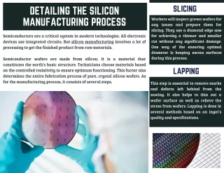
SLICING DETAILING THE SILICON MANUFACTURING PROCESS Workers will inspect grown wafers for any issues and prepare them for slicing. They use a diamond edge saw for achieving a thinner and smaller cut without any significant damage. One way of the ensuring optimal diameter is keeping excess surfaces during this process. Semiconductors are a critical system in modern technologies. All electronic devices use integrated circuits. But silicon manufacturing involves a lot of processing to get the finished product from raw materials. Semiconductor wafers are made from silicon. It is a material that constitutes the earth’s basic structure. Technicians choose materials based on the controlled resistivity to ensure optimum functioning. This factor also determines the entire fabrication process of pure, crystal silicon wafers. As for the manufacturing process, it consists of several steps. LAPPING This step is essential to remove marks and defects left behind from the sawing. It also helps to thin out a wafer surface as well as relieve the stress from wafers. Lapping is done in several methods based on an ingot’s quality and specifications.
POLISHING High-quality silicon wafers undergo multiple stages of polishing. It starts with a stock removal process to remove a thin layer of any silicon surface. Then, the second chemical mechanical polish step is performed to give a shiny and mirror finish. INGOT GROWTH Silicon production starts with growing ingots. This phase takes about one or several months based on the size, quality, and specifications. A well-known method of producing silicon is the Czocharlski method, where technicians add small quantities of dopants like Boron, Phosphorus, and Arsenic to silicon materials. Then, the mixture is heating above 1412 degrees Celsius, and crystals with the same orientation are placed inside to facilitate growth with minimal defects. CLEANING Once done with lapping, wafers require chemical etching and cleaning. It further allows technicians to fix any cracks or minor defects on wafers. Cleaning at microscopic levels is necessary for achieving high-quality products. Typically, a cleaning bath consists of sodium hydroxide, acetic acid, and nitric acid solutions. FL 33407 (561) 842-4441