
Computer Memory Organization
E N D
Presentation Transcript
Computer Organization15CS34Mr. Anand S. Hiremath,Dept. of CSE, BLDEA’s CET, Vijayapurhttp://ashiremath.wordpress.comashiremath@bldeacet.ac.in
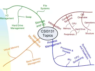
Module-3Memory • Basic memory circuits • Organization of the main memory • Memory technology • Cache memory, which reduces the effective memory access time • Virtual memory, which increases the apparent size of the main memory • Magnetic and optical disks used for secondary storage
Books to Refer • Text Books: • Carl Hamacher, ZvonkoVranesic, SafwatZaky: Computer Organization, 5th Edition, Tata McGraw Hill, 2002. • Carl Hamacher, ZvonkoVranesic, SafwatZaky, NaraigManjikian: Computer Organization and Embedded Systems, 6th Edition, Tata McGraw Hill, 2012. • Reference Books: • William Stallings: Computer Organization & Architecture, 9th Edition, Pearson, 2015.
Introduction • Execution speed of programs is highly dependent on the speed with which instructions and data can be transferred between the processor and the memory. • Ideally, the memory would be fast, large, and inexpensive. • Unfortunately, it is impossible to meet all three of these requirements simultaneously. Increased speed and size are achieved at increased cost. • Much work has gone into developing structures that improve the effective speed and size of the memory, yet keep the cost reasonable.
Basic Concepts-1 • The maximum size of the memory that can be used in any computer is determined by the addressing scheme. • For example, a computer that generates 16-bit addresses is capable of addressing up to 216= 64K (kilo) memory locations
Basic Concepts-2 • The memory is usually designed to store and retrieve data in word-length quantities. • Consider, for example, a byte-addressable computer whose instructions generate 32-bit addresses. • When a 32-bit address is sent from the processor to the memory unit, the high order 30 bits determine which word will be accessed. If a byte quantity is specified, the low-order 2 bits of the address specify which byte location is involved.
Basic Concepts-4 • The connection between the processor and its memory consists of address, data, and control lines,
Basic Concepts-5 • The processor uses the address lines to specify the memory location involved in a data transfer operation, and uses the data lines to transfer the data. • At the same time, the control lines carry the command indicating a Read or a Write operation and whether a byte or a word is to be transferred. The control lines also provide the necessary timing information and are used by the memory to indicate when it has completed the requested operation. • When the processor-memory interface receives the memory’s response, it asserts the MFC (Memory Function Complete) signal
Basic Concepts-6 • A useful measure of the speed of memory units is the time that elapses between the initiation of an operation to transfer a word of data and the completion of that operation. • This is referred to as the memory access time. • Another important measure is the memory cycle time, which is the minimum time delay required between the initiation of two successive memory operations, for example, the time between two successive Read operations. • The cycle time is usually slightly longer than the access time.
Basic Concepts-7 • A memory unit is called a random-access memory (RAM) if the access time to any location is the same, independent of the location’s address. • This distinguishes such memory units from serial, or partly serial, access storage devices such as magnetic and optical disks. • Access time of the latter devices depends on the address or position of the data.
Basic Concepts-8 • Cache and Virtual Memory • The processor of a computer can usually process instructions and data faster than they can be fetched from the main memory. Hence, the memory access time is the bottleneck in the system. • One way to reduce the memory access time is to use a cache memory. • This is a small, fast memory inserted between the larger, slower main memory and the processor. It holds the currently active portions of a program and their data. • Virtual memory With this technique, only the active portions of a program are stored in the main memory, and the remainder is stored on the much larger secondary storage device. Sections of the program are transferred back and forth between the main memory and the secondary storage device in a manner that is transparent to the application program. As a result, the application program sees a memory that is much larger than the computer’s physical main memory.
Semiconductor RAM Memories-1 • Internal Organization of Memory Chips
Semiconductor RAM Memories-2 • Memory cells are in the form of an array, in which each cell is capable of storing one bit of information. • Each row of cells constitutes a memory word, and all cells of a row are connected to a common line referred to as the word line, which is driven by the address decoder on the chip. • The cells in each column are connected to a Sense/Write circuit by two bit lines, and the Sense/Write circuits are connected to the data input/output lines of the chip. • During a Read operation, these circuits sense, or read, the information stored in the cells selected by a word line and place this information on the output data lines. • During a Write operation, the Sense/Write circuits receive input data and store them in the cells of the selected word.
Semiconductor RAM Memories-3 • In above example of a very small memory circuit consisting of 16 words of 8 bits each. • This is referred to as a 16 × 8 organization. • The data input and the data output of each Sense/Write circuit are connected to a single bidirectional data line that can be connected to the data lines of a computer. • The R/W (Read/Write) input specifies the required operation, and the CS (Chip Select) input selects a given chip in a multichip memory system.
Semiconductor RAM Memories-4 • Number of external connections required • The memory in above example stores 128 bits and requires 14 external connections for address (4), data(8), and control lines(2). It also needs two lines (2) for power supply and ground connections. • Now in case of 1K (1024) memory cells. This circuit can be organized as a 128 × 8 memory, requiring a total of 19 external connections. (7+8+2+2) • The same number of cells can be organized into a 1K×1 format. In this case, a 10-bit address is needed, but there is only one data line, resulting in 15 external connections. (10+1+2+2) • A 1G-bitchip may have a 256M × 4 organization, in which case a 28-bit address is needed and 4 bits are transferred to or from the chip. (28+4+2+2)
Semiconductor RAM Memories-5 • Organization of a 1K × 1 memory chip. • 10-bit address is divided into two groups of 5 bits each to form the row and column addresses for the cell array. • A row address selects a row of 32 cells, all of which are accessed in parallel. • But, only one of these cells is connected to the external data line, based on the column address
Semiconductor RAM Memories-6Static Memories (SRAM) • Memories that consist of circuits capable of retaining their state as long as power is applied are known as static memories.
Semiconductor RAM Memories-7Static Memories (SRAM) • Two inverters are cross-connected to form a latch. The latch is connected to two bit lines by transistors T1 and T2. These transistors act as switches that can be opened or closed under control of the word line. • When the word line is at ground level, the transistors are turned off and the latch retains its state. • For example, if the logic value at point X is 1 and at point Y is 0, this state is maintained as long as the signal on the word line is at ground level. Assume that this state represents the value 1.
Semiconductor RAM Memories-8Static Memories (SRAM) • Read Operation • Assume cell is in state 1. • To read keep Word line to 1. • So signal on bit line b is high and the signal on bit line b` is low
Semiconductor RAM Memories-9Static Memories (SRAM) • Write Operation • During a Write operation, the Sense/Write circuit drives bit lines b and b`. • It places the appropriate value on bit line b and its complement on b` and activates the word line. • This forces the cell into the corresponding state, which the cell retains when the word line is deactivated.
Semiconductor RAM Memories-10Static Memories (SRAM) • CMOS Cell • Transistor pairs (T3, T5) and (T4, T6) form the inverters in the latch. • The state of the cell is read or written as just explained. For example, in state 1, the voltage at point X is maintained high by having transistors T3 and T6 on, while T4 and T5 are off. • If T1 and T2 are turned on, bit lines b and b`will have high and low signals, respectively.
Semiconductor RAM Memories-11Static Memories (SRAM) • Continuous power is needed for the cell to retain its state. If power is interrupted, the cell’s contents are lost. When power is restored, the latch settles into a stable state, but not necessarily the same state the cell was in before the interruption. Hence, SRAMs are said to be volatile memories. • A major advantage of CMOS SRAMs is their very low power consumption, because current flows in the cell only when the cell is being accessed. • Static RAMs can be accessed very quickly. Access times on the order of a few nanoseconds are found in commercially available chips. SRAMs are used in applications where speed is of critical concern.
Semiconductor RAM Memories-12Asynchronous Memories (DRAM) • Static RAMs are fast, but their cells require several transistors. • Less expensive and higher density RAMs can be implemented with simpler cells. • But, these simpler cells do not retain their state for a long period, unless they are accessed frequently (Refreshed) for Read or Write operations. • Memories that use such cells are called dynamic RAMs (DRAMs).
Semiconductor RAM Memories-13Asynchronous Memories (DRAM) • Information is stored in a dynamic memory cell in the form of a charge on a capacitor, but this charge can be maintained for only tens of milliseconds. • Since the cell is required to store information for a much longer time, its contents must be periodically refreshed (read or write) by restoring the capacitor charge to its full value.
Semiconductor RAM Memories-14Asynchronous Memories (DRAM) • A single-transistor dynamic memory cell. • To store information in this cell, transistor T is turned on and an appropriate voltage is applied to the bit line. • This causes a known amount of charge to be stored in the capacitor. • After the transistor is turned off, the charge remains stored in the capacitor, but not for long. The capacitor begins to discharge.
Semiconductor RAM Memories-15Asynchronous Memories (DRAM) • This is because the transistor continues to conduct a tiny amount of current, after it is turned off. • Hence, the information stored in the cell can be retrieved correctly only if it is read before the charge in the capacitor drops below some threshold value. • During a Read operation, the transistor in a selected cell is turned on. • A sense amplifier connected to the bit line detects whether the charge stored in the capacitor is above or below the threshold value. • If the charge is above the threshold, the sense amplifier drives the bit line to the full voltage representing the logic value 1. As a result, the capacitor is recharged. • If the sense amplifier detects that the charge in the capacitor is below the threshold value, it pulls the bit line to ground level to discharge the capacitor fully. • Thus, reading the contents of a cell automatically refreshes its contents. • Since the word line is common to all cells in a row, all cells in a selected row are read and refreshed at the same time.
Semiconductor RAM Memories-16Asynchronous Memories (DRAM) • Internal organization of a 2M × 8 dynamic memory chip.
Semiconductor RAM Memories-17Asynchronous Memories (DRAM) • A 16-Megabit DRAM chip, configured as 2M × 8, is shown in above diagram. • The cells are organized in the form of a 4K × 4K array. • The 4096 cells in each row are divided into 512 groups of 8, forming 512 bytes of data. • Therefore, 12 address bits are needed to select a row, and another 9 bits are needed to specify a group of 8 bits in the selected row. • In total, a 21-bit address is needed to access a byte in this memory. • The high-order 12 bits and the low-order 9bits of the address constitute the row and column addresses of a byte, respectively. • To reduce the number of pins needed for external connections, the row and column addresses are multiplexed on 12 pins.
Semiconductor RAM Memories-18Asynchronous Memories (DRAM) • During a Read or a Write operation, the row address is applied first. • It is loaded into the row address latch in response to a signal pulse on an input control line called the Row Address Strobe (RAS). • This causes a Read operation to be initiated, in which all cells in the selected row are read and refreshed.
Semiconductor RAM Memories-19Asynchronous Memories (DRAM) • Shortly after the row address is loaded, the column address is applied to the address pins and loaded into the column address latch under control of a second control line called the Column Address Strobe (CAS). • The information in this latch is decoded and the appropriate group of 8 Sense/Write circuits is selected. • If the R/W control signal indicates a Read operation, the output values of the selected circuits are transferred to the data lines, D7−D0. • For a Write operation, the information on the D7−D0 lines is transferred to the selected circuits, then used to overwrite the contents of the selected cells in the corresponding 8 columns. • We should note that in commercial DRAM chips, the RAS and CAS control signals are active when low.
Semiconductor RAM Memories-20Asynchronous Memories (DRAM) • The timing of the operation of the DRAM described above is controlled by the RAS and CAS signals. • These signals are generated by a memory controller circuit external to the chip when the processor issues a Read or a Write command. • During a Read operation, the output data are transferred to the processor after a delay equivalent to the memory’s access time. • Such memories are referred to as asynchronous DRAMs. • The memory controller is also responsible for refreshing the data stored in the memory chips.
Semiconductor RAM Memories-21Asynchronous Memories (DRAM) • Fast Page Mode • When the DRAM in above example is accessed, the contents of all 4096 cells in the selected row are sensed, but only 8 bits are placed on the data lines, D7−D0. This byte is selected by the column address, bits A8−0. • A simple addition to the circuit makes it possible to access the other bytes in the same row without having to reselect the row. • Each sense amplifier also acts as a latch. • When a row address is applied, the contents of all cells in the selected row are loaded into the corresponding latches. • Then, it is only necessary to apply different column addresses to place the different bytes on the data lines.
Semiconductor RAM Memories-22Asynchronous Memories (DRAM) • This arrangement leads to a very useful feature. All bytes in the selected row can be transferred in sequential order by applying a consecutive sequence of column addresses under the control of successive CAS signals. • Thus, a block of data can be transferred at a much faster rate than can be achieved for transfers involving random addresses. • This feature is referred to as the fast page mode. (A large block of data is often called a page.)
Semiconductor RAM Memories-23Synchronous DRAMs (SDRAM) • DRAMs whose operation is synchronized with a clock signal. Such memories are known as synchronous DRAMs (SDRAMs). • The cell array is the same as in asynchronous DRAMs. • SDRAMs have built-in refresh circuitry, with a refresh counter to provide the addresses of the rows to be selected for refreshing. • As a result, the dynamic nature of these memory chips is almost invisible to the user.
Semiconductor RAM Memories-25Synchronous DRAMs(SDRAM) • SDRAMs have several different modes of operation, which can be selected by writing control information into a mode register. • For example, in burst operations of different lengths can be specified. • It is not necessary to provide externally-generated pulses on the CAS line to select successive columns. • The necessary control signals are generated internally using a column counter and the clock signal. • New data are placed on the data lines at the rising edge of each clock pulse.
Semiconductor RAM Memories-26Synchronous DRAMs(SDRAM) • Timing diagram for a typical burst read of length 4
Semiconductor RAM Memories-27Synchronous DRAMs(SDRAM) • First, the row address is latched under control of the RAS signal. The memory typically takes 2 or 3 clock cycles (we use 2 in the figure for simplicity) to activate the selected row. Then, the column address is latched under control of the CAS signal. • After a delay of one clock cycle, the first set of data bits is placed on the data lines. • The SDRAM automatically increments the column address to access the next three sets of bits in the selected row, which are placed on the data lines in the next 3 clock cycles.
Semiconductor RAM Memories-28Synchronous DRAMs(SDRAM) • Synchronous DRAM scan deliver data at a very high rate, because all the control signals needed are generated inside the chip. • The initial commercial SDRAMs designed for clock speeds of up to 133 MHz. • As technology evolved, much faster SDRAM chips were developed. Today’s SDRAMs operate with clock speeds that can exceed 1 GHz.
Semiconductor RAM Memories-28Synchronous DRAMs(SDRAM) • Latency and Bandwidth • Data transfers to and from the main memory often involve blocks of data. • The memory access time defined earlier is not sufficient for describing the memory’s performance when transferring blocks of data. During block transfers, memory latency is the amount of time it takes to transfer the first word of a block. • The time required to transfer a complete block depends also on the rate at which successive words can be transferred and on the size of the block. The time between successive words of a block is much shorter than the time needed to transfer the first word. • For instance, as in the timing diagram, the access cycle begins with the assertion of the RAS signal. The first word of data is transferred five clock cycles later. Thus, the latency is five clock cycles. If the clock rate is 500 MHz, then the latency is 10 ns. • The remaining three words are transferred in consecutive clock cycles, at the rate of one word every 2 ns.
Semiconductor RAM Memories-29Synchronous DRAMs(SDRAM) • A useful performance measure is the number of bits or bytes that can be transferred in one second. This measure is referred as the memory bandwidth. • It depends on the speed of access to the stored data and on the number of bits that can be accessed in parallel. • The rate at which data can be transferred to or from the memory depends on the bandwidth of the system interconnections. • For this reason, the interconnections used always ensure that the bandwidth available for data transfers between the processor and the memory is very high.
Semiconductor RAM Memories-30Synchronous DRAMs • Double-Data-Rate SDRAM (DDR-RAM) • The key idea is to take advantage of the fact that a large number of bits are accessed at the same time inside the chip when a row address is applied. • To make the best use of the available clock speed, data are transferred externally on both the rising and falling edges of the clock. • For this reason, memories that use this technique are called double-data-rate SDRAMs (DDR SDRAMs).
Semiconductor RAM Memories-31Synchronous DRAMs • Several versions of DDR chips have been developed. The earliest version is known as DDR. Later versions, called DDR2, DDR3, and DDR4, have enhanced capabilities. • They offer increased storage capacity, lower power, and faster clock speeds. • For example, DDR2 and DDR3 can operate at clock frequencies of 400 and 800 MHz, respectively. Therefore, they transfer data using the effective clock speeds of 800 and 1600 MHz, respectively.
Semiconductor RAM Memories-32Structure of Larger Memories • The basic organization of memory circuits as they may be implemented on a single chip. Now examine how memory chips may be connected to form a much larger memory.
Semiconductor RAM Memories-33Structure of Larger Memories • Static Memory Systems • Consider a memory consisting of 2M words of 32 bits each. Shown in next slide, how this memory can be implemented using 512K × 8 static memory chips. • Each column in the figure implements one byte position in a word, with four chips providing 2M bytes. • Four columns implement the required 2M × 32 memory.
Semiconductor RAM Memories-34Structure of Larger Memories • Each chip has a control input called Chip-select. When this input is set to 1, it enables the chip to accept data from or to place data on its data lines.
Semiconductor RAM Memories-35Structure of Larger Memories • Organization of a 2M × 32 memory module using 512K × 8 static memory chips.
Semiconductor RAM Memories-36Structure of Larger Memories • Only the selected chip places data on the data output line, while all other outputs are electrically disconnected from the data lines. • 21 address bits are needed to select a 32-bit word in this memory. • The high-order two bits of the address are decoded to determine which of the four rows should be selected. • The remaining 19 address bits are used to access specific byte locations inside each chip in the selected row. • The R/W inputs of all chips are tied together to provide a common Read/Write control line (not shown in the figure).
Semiconductor RAM Memories-37Structure of Larger Memories • Dynamic Memory Systems • Modern computers use very large memories. Even a small personal computer is likely to have at least 1G bytes of memory. Typical desktop computers may have 4G bytes or more of memory. • A large memory leads to better performance, because more of the programs and data used in processing can be held in the memory, thus reducing the frequency of access to secondary storage.