Application of APD Arrays in Photon Counting: Fabrication and Optimization
Learn about single-photon measurement devices for ghost imaging, fabrication of 2-D APD arrays, and principles of chemical detection with lasers for remote sensing applications. Discover the key requirements for photon counting and optimization techniques for APD arrays. Explore mesa vs. guard-ring APDs, reliability testing, and design considerations for achieving high differential gain and low dark current.

Application of APD Arrays in Photon Counting: Fabrication and Optimization
E N D
Presentation Transcript
Quantum Imaging -UMBC Part IV Single-photon measurement device for “ghost” imaging - Fabrication of individual addressable 2-D APD arrays
MOCVD Laboratories Reactor I Reactor II Cleanroom Cleanroom
Reasons To Select APD for Photon Counting • Possible to achieve large arrays with good uniformity. • Possible to obtain good photon counting performance at TE cooler chilled temperatures. • Infrastructure for commercialization exists.
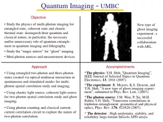
Remote Sensing - Imaging Lidar Prof. Ray Hoff, UMBC, NASA JCET Center
. . . . . . IR LASER TRANSMITTER AND RECEIVER . . Principles of Chemical Detection with Lasers DIfferential SCattering/DIfferential Absorption Lidar (DISC/DIAL) • Rapidly tuned laser emits 2 or more wavelengths that penetrate cloud • Light is differentially absorbed/scattered upon transmission as well as reflection • Light reflects off of topographic/aerosol/rain targets & detected at receiver • Agents identified since each has a unique absorption/scattering spectrum
Key Requirements for Photon Counting (PC) 1. Low Dark Counts: Dark current is caused by surface leakage, tunneling, defects assisted tunneling. Can be reduced by decrease the electrical field in the active (absorption) region. 2. High Gain and High Differential Gain High gain can be obtained with high bias voltage. However, with high bias, a high dark current will also be produced. High differential gain relies on high rising slope of APD (dG/dV). An ideal PC APD will have a straight angle I-V curve, which can be achieved with better device designs. 3. Designing and Fabricating Materials with Reduced After-Pulse Dark Current (AFDC) Amplitude and Duration AFDC comes from traps in the avalanche regions and trapped carriers in the hetero-interface. Interstitial Zn atoms created during the diffusion processes are source of traps and can be activated and converted to substitutional dopants by appropriate annealing procedures. More steps of InGaAsP quaternary layers (1.1Q, 1.2Q, 1.3Q, 1.5Q, ..etc.) can added to the InP/InGaAs interface to reduce hole trapping.
Etch-Mesa Surface Leakage Current Studies Annealing with 300°C Polyimide passivation With H2SO4 treatment H2SO4 surface treatment can reduce the surface leakage current, However, after add in polyimide passivation the surface leakage current increases.
Mesa structure APDs are the current state-of-the-art Potential issues with mesa APDS for space applications: Short lifetime from early breakdown Dark current increases over time We are focusing on guard-ring designs to address the above issues Mesa vs. Guard-Ring Mesa Guard-Ring
Reliability of Guard-Ring APDS Aging test condition: 200oC/I=100A Testing method: measure dark current at M~10 periodically * S. Tanaka et al on OFC 2003
P doping Guard Ring Type High Stability and High Reliability APDs
d1 d2 Optimize Design To Achieve High Differential Gain and Low Dark Current Changing the avalanche region thickness, d1, the charging layer Doping and thickness d2 will greatly affect the APD characteristics Lower dark current and high diff gain can be achieved
Vp VB Reducing Tunneling Leakage Current Reducing the distance between the punch through voltage and the breakdown voltage will help to reduce the voltage drop falling on the small bandgap absorption region Breakdown field (V/cm) for InP is around 5e5 (handbook series on semiconductor parameters); and for InGaAs is 2e5.
d1=400 nm d1=200 nm Summary of Calculated Results
Dark Current I-V Characteristics Changing with Temperature * The dark current is reduced • The gain is increased • A sharp rising gain with the bias voltage will help to choose good operating points.
4x4 Photon Counting APD Arrays and Their I-V Characteristics
CAPD R// 1 R// 2 Determined by the avalanche process and is not sensitive to ext. Circuits Determined by T= R// *CAPD Photon Counting Operations I Current Source
Photon Counting Pulse Amplitude Statistics IDC=0.005 µA, Vac=4.0 V IDC=0.007 µA, Vac=4.0 V