Download
1 / 12
120 likes | 247 Vues
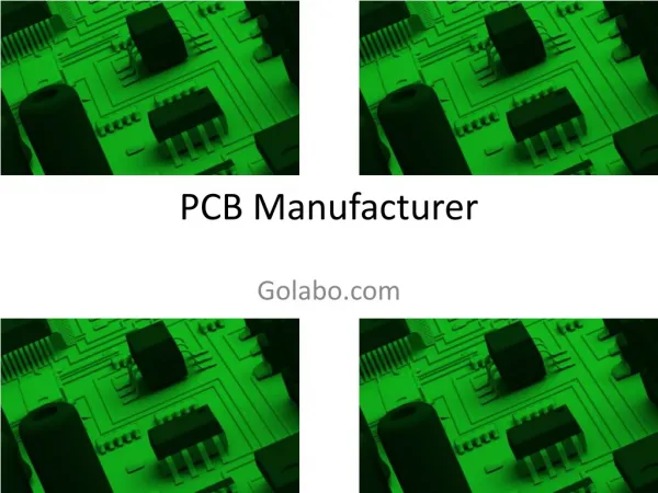
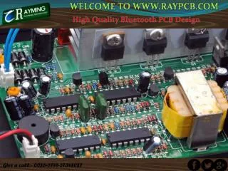
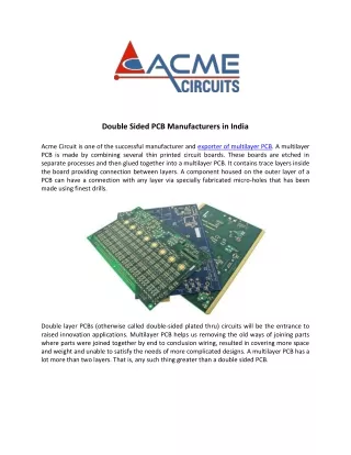
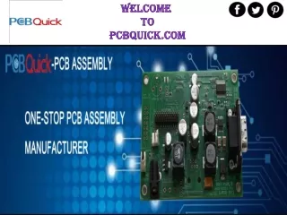
Useful Links<br>http://pageantiques.com.au/<br>http://narromineshiredentalsurgery.com.au/<br>http://parkbeachdentalsurgery.com.au<br>http://www.triodepcb.com/<br><br>PCB Manufacturer<br> A PCB is printed circuit board, also known as a printed wiring board. It is used in electronics to build electronic devices. A PCB serves 2 purposes in the construction of an electronic device. It is a place to mount the components it provides the means of electrical connection between the components.<br> A PCB populated with the electronic components and is a printed circuit assembly(PCA),also known as a printed circuit board assembly(PCBA).<br>Steps in PCB Circuit Board Manufacturing<br>1)Film Generation<br> Films for all of the copper and soldermask layers are made from photographically exposed mylar.<br>2)Select Raw Material<br> Industry standard 0.059" thick FR-4 laminate copper clad on two sides.<br>3)Drill Holes<br> Through holes required are created from your submitted files for your PCB design, using NC drill machines and carbide drill bits.<br>4)Electroless Copper<br> In order for the through holes to electrically connect to the different layers of the PCB,a thin layer of copper is a chemically deposited into the through holes. This copper will later be thickened through electrolytic copper plating.<br>5)Apply Photo-resist and Image<br> To transfer the PCB design from the electronic CAD data to the physical circuit board. 6)Pattern Plate<br> This step is an electrochemical process which builds copper thickness into the holes and onto the surface of the PCB.<br>7)Strip & Etch<br> This process takes place in multiple steps.The first is to chemically remove the photo resist from the panel.<br>8)Soldermask<br> Next we coat the entire panel with a liquid soldermask layer.Using films and high intensity UV light we expose the solderable areas of the PCB.<br>9)Nomenclature(silkscreen)<br> Next we print the reference designators, logos and the other information contained in the electronic files,onto the panel.<br>10)Surface Finish Applied<br> This surface finish is used to protect the copper from oxidation as well as a site for soldering of components to the PCB.<br>11)Fabrication<br> We route the perimeter of the PCB from the larger panel using NC equipment.<br> We can assemble up to 400mm*400mm without any difficulty. We can provide a DFM report for all new products assembled at Triode.If you would like a pre-job review, contact us and one of our Process Engineers will review your products.

E N D
Introduction A PCB is printed circuit board, also known as a printed wiring board. It is used in electronics to build electronic devices. A PCB serves 2 purposes in the construction of an electronic device. It is a place to mount the components it provides the means of electrical connection between the components.
A PCB populated with the electronic components and is a printed circuit assembly(PCA),also known as a printed circuit board assembly(PCBA).
Steps in PCB Circuit Board Manufacturing 1) Film Generation 2) Select Raw Material 3) Drill Holes 4) ElectrolessCopper 5) Apply Photo-resist and Image 6) Pattern Plate 7) Strip & Etch 8)Soldermask 9)Nomenclature(silkscreen) 10)Surface Finish Applied 11)Fabrication
2) Select Raw Material 1) Film Generation 3)Drill Holes
Steps in PCB Circuit Board Manufacturing 1)Film Generation Films for all of the copper and soldermask layers are made from photographically exposed mylar. 2)Select Raw Material Industry standard 0.059" thick FR-4 laminate copper clad on two sides. 3)Drill Holes Through holes required are created from your submitted files for your PCB design, using NC drill machines and carbide drill bits. 4)Electroless Copper In order for the through holes to electrically connect to the different layers of the PCB,a thin layer of copper is a chemically deposited into the through holes. This copper will later be thickened through electrolytic copper plating. 5)Apply Photo-resist and Image To transfer the PCB design from the electronic CAD data to the physical circuit board. 6)Pattern Plate This step is an electrochemical process which builds copper thickness into the holes and onto the surface of the PCB.
4) Electroless Copper 5) Apply Photo-resist and Image 6) Pattern Plate
7)Strip & Etch This process takes place in multiple steps.The first is to chemically remove the photo resist from the panel. 8)Soldermask Next we coat the entire panel with a liquid soldermasklayer.Using films and high intensity UV light we expose the solderable areas of the PCB. 9)Nomenclature(silkscreen) Next we print the reference designators, logos and the other information contained in the electronic files,onto the panel. 10)Surface Finish Applied This surface finish is used to protect the copper from oxidation as well as a site for soldering of components to the PCB. 11)Fabrication We route the perimeter of the PCB from the larger panel using NC equipment. We can assemble up to 400mm*400mm without any difficulty. We can provide a DFM report for all new products assembled at Triode.If you would like a pre-job review, contact us and one of our Process Engineers will review your products.
7) Strip & Etch 8)Soldermask 9)Nomenclature(silkscreen)
10)Surface Finish Applied 11)Fabrication
TRIODE GROUP LIMITED purchases the business products of Precision Manufacturing Solutions Ltd