Download
1 / 32
460 likes | 1.16k Vues
ADC & DAC. Signal Conversions. Conversion scenario. A/D Analogue to Digital Converter. Resolution:

E N D
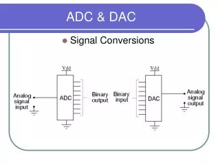
ADC & DAC • Signal Conversions
A/D Analogue to Digital Converter Resolution: The resolution of the converter indicates the number of discrete values it can produce over the range of analog values. The values are usually stored electronically in binary form, so the resolution is usually expressed in bits. In consequence, the number of discrete values available, or "levels", is usually a power of two. For example, an ADC with a resolution of 8 bits can encode an analog input to one in 256 different levels, since28 = 256. The values can represent the ranges from 0 to 255 (i.e. unsigned integer) or from -128 to 127 (i.e. signed integer), depending on the application.
A/D Analogue to Digital Converter • Resolution can also be defined electrically, and expressed in volts. The voltage resolution of an ADC is equal to its overall voltage measurement range divided by the number of discrete intervals as in the formula: • Where: • Q is resolution in volts per step (volts per output codes less one), • EFSR is the full scale voltage range = VRefHi − VRefLow, • M is the ADC's resolution in bits. • N is the number of intervals, (one less than the number of available levels, or output codes), which is: N = 2M − 1
A/D Analogue to Digital Converter Example 1: • Full scale measurement range = 0 to 10 volts • ADC resolution is 12 bits: 212 = 4096 quantization levels (codes) • ADC voltage resolution is: (10V - 0V) / 4095 steps = 10V / 4095 steps 0.00244 V/step 2.44 mV/step
A/D Analogue to Digital Converter Example 2 • Full scale measurement range = -10 to +10 volts • ADC resolution is 14 bits: 214 = 16384 quantization levels (codes) • ADC voltage resolution is: (10V - (-10V)) / 16383 steps = 20V / 16383 steps 0.00122 V/step 1.22 mV/step
A/D Analogue to Digital Converter Example 3 • Full scale measurement range = 0 to 7 volts • ADC resolution is 3 bits: 23 = 8 quantization levels (codes) • ADC voltage resolution is: (7 V − 0 V)/7 steps = 7 V/7 steps = 1 V/ step = 1000 mV/step
Flash Method A/D Converter Circuit for 2-bit A/D The heart of a Flash analog to digital converter is a set of resistors strung together in series. This so-called resistor ladder equally divides an input voltage across each resistor . Thus, a 1-volt input across a 4-resistor ladder will result in 0.25 volts developing across each resistor (see Figure ). An input analog voltage can then be compared in parallel against this reference voltage ladder using an array of 1-bit quantizers.
Flash Method A/D Converter The resulting digital output is coded in a form called a “thermometer code”, where the output value is equal to the length of consecutive 1’s in the code. So in this example: • binary thermometer • 00 0000 • 01 0001 • 0011 • 11 01 • * 1111 [overflow condition]
Flash Method A/D Converter Vref is a stable reference voltage provided by a precision voltage regulator as part of the converter circuit, not shown in the schematic. As the analog input voltage exceeds the reference voltage at each comparator, the comparator outputs will sequentially saturate to a high state. The priority encoder generates a binary number based on the highest-order active input, ignoring all other active inputs
Flash Method A/D Converter • This converter is extremely fast because the entire conversion happens in a single wide parallel conversion operation, as opposed to the sigma delta/oversampled or successively approximated methods used in other converters. This architecture has some significant drawbacks, however, including: • Resolution limited by quality of resistor ladder (resistors must be accurate to better than 1/2n, such that an 8-bit converter requires better than 0.5% matched resistors) • 2n quantizers required for an n-bit output • Relatively high power consumption
successive approximation ADC A successive approximation ADC is a type of analog-to-digital converter that converts a continuous analog waveform into a discrete digitalrepresentation via a binary search through all possible quantization levels before finally converging upon a digital output for each conversion
successive approximation ADC Algorithm: • The successive approximation Analog to digital converter circuit typically consists of four chief subcircuits: • A sample and hold circuit to acquire the input voltage (Vin). • An analog voltage comparator that compares Vin to the output of the internal DAC and outputs the result of the comparison to the successive approximation register (SAR). • A successive approximation register subcircuit designed to supply an approximate digital code of Vin to the internal DAC. • An internal reference DAC that supplies the comparator with an analog voltage equivalent of the digital code output of the SAR for comparison with Vin.
Successive Method of A/D Converter Sampling Sampling refers to the extraction of signals at given intervals of time. In the case of digital sampling, whether the digital signal is high or low level is determined, and this information is used to trigger circuit operation. In communication, the sampling is done to recognize whether the receive data is "1" or "0" Analog clock sampling is performed to convert the analog signal voltage into a digital value with an A/D converter.
Successive Method of A/D Converter In order to process the analog signals in the natural world as digital signals in a microcontroller, an A/D (analog to digital) converter is required. Most of today's microcontrollers contain A/D converters on the microcontroller chip. The A/D converter captures analog signals at fixed time intervals along the time axis. This process is known as sampling, and the fixed time interval is known as the sampling period (the inverse of the sampling period is called the sampling frequency). On the other hand, the approaching of a predetermined discrete value along the amplitude axis is known as quantization.
Successive Method of A/D Converter The following points must be observed when carrying out A/D conversion.(1) Caution concerning the relationship between the sampling frequency and the analog signal frequencyThe sampling frequency (fs) must be at least twice the analog signal frequency (f) (Shannon's sampling theorem). For example, when the analog signal frequency and the sampling frequency are the same, as shown in the figure given, the value after digital conversion is always constant, making it impossible for the digital waveform to approximate the analog waveform
Successive Method of A/D Converter The following figure shows the waveforms when the sampling frequency (fs) is twice the analog signal frequency (f). At twice the frequency, the digital waveform at last becomes a triangular waveform with the same frequency as the analog signal frequency. When the waveform phases are out of alignment, the amplitude becomes smaller. In this case, a large error occurs unless the sampling frequency is made even larger than twice the frequency of the analog waveform.It is therefore necessary to select an A/D converter of the conversion speed to execute sampling at a frequency that is at least twice the upper limit of the frequency of the analog signal to be converted to the digital signal.
Successive Method of A/D Converter When the A/D converter is converting analog signals to digital signals, the analog signals are not steady; they are always changing. Because of this, in order to obtain accurate conversion values, it is necessary to put a sample & hold circuit in the stage just before the A/D converter to hold the analog signals steady for conversion. This sample & hold circuit is now commonly found in microcontrollers.
Successive Method of A/D Converter Throughout the count process, the register monitors the comparator's output to see if the binary count is less than or greater than the analog signal input, adjusting the bit values accordingly. The way the register counts is identical to the "trial-and-fit" method of decimal-to-binary conversion, whereby different values of bits are tried from MSB to LSB to get a binary number that equals the original decimal number. The advantage to this counting strategy is much faster results: the DAC output converges on the analog signal input in much larger steps than with the 0-to-full count sequence of a regular counter.
Successive Method of A/D Converter It should be noted that the SAR is generally capable of outputting the binary number in serial (one bit at a time) format, thus eliminating the need for a shift register. Plotted over time, the operation of a successive-approximation ADC looks like this:
ΔΣ converter In a ΔΣ converter, the analog input voltage signal is connected to the input of an integrator, producing a voltage rate-of-change, or slope, at the output corresponding to input magnitude. This ramping voltage is then compared against ground potential (0 volts) by a comparator. The comparator acts as a sort of 1-bit ADC, producing 1 bit of output ("high" or "low") depending on whether the integrator output is positive or negative. The comparator's output is then latched through a D-type flip-flop clocked at a high frequency, and fed back to another input channel on the integrator, to drive the integrator in the direction of a 0 volt output. The basic circuit looks like this
ΔΣ converter • If the integrator output is positive, the first comparator will output a "high" signal to the D input of the flip-flop. At the next clock pulse, this "high" signal will be output from the Q line into the noninverting input of the last comparator. This last comparator, seeing an input voltage greater than the threshold voltage of 1/2 +V, saturates in a positive direction, sending a full +V signal to the other input of the integrator. This +V feedback signal tends to drive the integrator output in a negative direction. If that output voltage ever becomes negative, the feedback loop will send a corrective signal (-V) back around to the top input of the integrator to drive it in a positive direction. This is the delta-sigma concept in action: the first comparator senses a difference (Δ) between the integrator output and zero volts. The integrator sums (Σ) the comparator's output with the analog input signal.
ΔΣ converter Functionally, this results in a serial stream of bits output by the flip-flop. If the analog input is zero volts, the integrator will have no tendency to ramp either positive or negative, except in response to the feedback voltage. In this scenario, the flip-flop output will continually oscillate between "high" and "low," as the feedback system "hunts" back and forth, trying to maintain the integrator output at zero volts:
ΔΣ converter By applying a larger (negative) analog input signal to the integrator, we force its output to ramp more steeply in the positive direction. Thus, the feedback system has to output more 1's than before to bring the integrator output back to zero volts:
ΔΣ converter As the analog input signal increases in magnitude, so does the occurrence of 1's in the digital output of the flip-flop:
ΔΣ converter A parallel binary number output is obtained from this circuit by averaging the serial stream of bits together. For example, a counter circuit could be designed to collect the total number of 1's output by the flip-flop in a given number of clock pulses. This count would then be indicative of the analog input voltage.
The R/2nR DAC • Summing currents circuit
The R/2nR DAC • 3 Bits DAC
The R/2nR DAC • Input with gates