Multi-Stage TIA Design: RF Circuit Analysis & Simulation Homework
This homework assignment focuses on the design, analysis, and simulation of a multi-stage Transimpedance Amplifier (TIA) for RF applications. Students will explore circuit architecture, perform DC/AC/noise analyses, simulate performance using HSPICE, and more. The report will compare results with target specifications, highlighting pros and cons.

Multi-Stage TIA Design: RF Circuit Analysis & Simulation Homework
E N D
Presentation Transcript
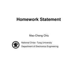
Homework Statement Mao-Cheng Chiu National Chiao -Tung University Department of Electronics Engineering
Outline • Specification of the TIA • Format of report • Topology examples • Using HSPICE to Analyze Performance
Report Outline • Design Homework • Circuit Architecture • Circuit Analysis • Simulation • DC/AC/Noise/Eye diagrams (for sensitivity and overload levels) • Summary • Comparison with target spec. • Pros & Cons
RF Examples of Multi-Stage TIA S. Yamashita, et al., IEEE JSSC, July. 2002 M. Ingels, et al., IEEE JSSC, Dec. 1994
AC analysis • Example: Is 0 1 ac 1 .ac dec 10 1k 5g .meas ac midgain FIND vdb(vo) AT=100MegHz .meas ac bandwidth when vdb(vo)='midgain-3.0' FALL=1 .meas ac maxgain max vdb(vo) Input signal AC analysis .probe Gain= par('vdb(vo)-idb(Is)') + phase= par('vp(vo)-ip(Is)') Gain & bandwidth .noise v(vo) Is 1 total equivalent input referred noise from 1k to 5g • BER= 10-12 =Q(Iin,pp/2In,in,rms) Iin,pp/2In,in,rms =7 Iinpp = 14 In,in,rms = Sensitivity
AC analysis • Simulation result: Sensitivity = Iinpp = 14 In,in,rms = 14* 0.264uA =3.7uA
PRBS Pattern 0 0 1 1 1 …. • Example: 2.5Gb/s K28.5 pattern ---00111110101100000101----- .param h = 50u Iin 0 g1 pwl( +0.00ns h +0.20ns 0 0.800ns 0 +1.00ns h 2.800ns h +3.00ns 0 3.200ns 0 +3.40ns h 3.600ns h +3.80ns 0 4.000ns 0 +4.20ns h 4.800ns h +5.00ns 0 6.800ns 0 +7.00ns h 7.200ns h +7.40ns 0 7.600ns 0 +7.80ns h 8.000ns h +R 0) 0.4ns • Rise time and fall time are both half of the bit time. • K28.5 contains five consecutive 1’s and five consecutive 0’s. • “h” is the magnitude of the input signal.
Eye Diagram • Example: .param width_eye =1.6ns phase=0ns .probe tran TIME_1.25G=par('TIME+phase-int((TIME+phase)/width_eye)*width_eye') Phase Width_eye • X-Axis = TIME_1.25G
Jitter & Overload • Measurement of Jitter : Jitter (p-p) Iin,pp= 3.7u ,Vout,pp= 5.1mV • Overload: Increases the input level and then check the output signal in the eye diagram. Iin,pp= 370u , Vout,pp= 0.52V Iin,max = overload