Download
1 / 43
430 likes | 587 Vues
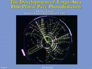
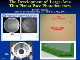
.075” ~150 20 m pores . INCOM glass substrate. The Development of Large-Area Thin Planar Psec Photodetectors. Henry Frisch, Enrico Fermi Institute UC and HEPD, ANL . SSL. SSL. Herve Grabas. The Large-Area Psec Photo-detector Collaboration.

E N D
.075” ~150 20m pores INCOM glass substrate The Development of Large-Area Thin Planar Psec Photodetectors Henry Frisch, Enrico Fermi Institute UC and HEPD, ANL SSL SSL Herve Grabas
The Large-Area Psec Photo-detector Collaboration 3 National Labs, 6 Divisions at Argonne, 3 US small companies, 3 universities Goal of 3-year R&D- commercializable modules. Fred Borcherding HEPD Visit
Three Goals of a New (1 yr-old) Collaborative Effort: • Large-Area Low-Cost Photodetectors with good correlated time and space resolution (target 10 $/sq-in incremental areal cost) • Large-Area TOF particle/photon detectors with psec time resolution ( < 1psec at 100 p.e.) • Understanding photocathodes so that we can reliably make high QE, tailor the spectral response, and develop new materials and geometries (QE > 50%, public formula) Fred Borcherding HEPD Visit
PET (UC/BSD, UCB, Lyon) Collider (UC, ANL,Saclay. Mass Spec Security (TBD) DUSEL (Matt, Mayly, Bob, John, ..) K->pnn (UC(?)) Parallel Efforts on Specific Applications Explicit strategy for staying on task . LAPD Detector Development Muon Cooling Muons,Inc (SBIR) ANL,Arradiance,Chicago,Fermilab, Hawaii,Muons,Inc,SLAC,SSL/UCB, Synkera, U. Wash. Drawing Not To Scale (!) All these need work- naturally tend to lag the reality of the detector development Fred Borcherding HEPD Visit
At colliders we measure the 3-momenta of hadrons, but can’t follow the flavor-flow of quarks,the primaryobjects that are colliding. 2-orders-of-magnitude in time resolution would all us to measure ALL the information=>greatly enhanced discovery potential. Application 1-Colliders A real top candidate event from CDF- has top, antitop, each decaying into a W-boson and a b or antib. Goal- identify the quarks that make the jets. (explain why…) Specs: Signal: 50-10,000 photons Space resolution: 1 mm Time resolution 1 psec Cost: <100K$/m2: t-tbar -> W+bW-bbar-> e+ nu+c+sbar+b+bbar
Application 2- Neutrino Physics • Spec: signal single photon, 100 ps time, 1 cm space, low cost/m2 (5-10K$/m2)* (Howard Nicholson) Fred Borcherding HEPD Visit
Application 3- Medical Imaging (PET) Alternating radiator and cheap 30-50 psec planar mcp-pmt’s on each side Can we solve the depth-of-interaction problem and also use cheaper faster radiators? Depth in crystal by time-difference Simulations by Heejong Kim (Chicago) Heejong Kim Heejong Kim Depth in crystal by energy- asymmetry Fred Borcherding HEPD Visit
Application 4- Cherenkov-sensitive Sampling Calorimeters A picture of an em shower in a cloud-chamber with ½” Pb plates (Rossi, p215- from CY Chao) Idea: planes on one side read both Cherenkov and scintillation light- on other only scintillation. • I A `cartoon’ of a fixed target geometry such as for JPARC’s KL-> pizero nunubar (at UC, Yao Wah) or LHCb Fred Borcherding HEPD Visit
Application 5- Nuclear Non-proliferation • MCP’s loaded with Boron or Gadolinium are used as neutron detectors with good gamma separation (Nova Scientific). • Large-area means could scan trucks, containers • Time resolution corresponds to space resolution out of the detector plane IF one has a t_0– i.e can do 3D tomography of objects Specs: TBD An area for possible applications- need a counterpart to form an application group. (ANL an obvious place) Fred Borcherding HEPD Visit
Detector Prescription (Generic) • Small feature size << 300 microns (1 inch = 1 nsec, 300 microns=1 psec) • Homogeneity – the ability to make uniform large-areas (think solar-panels, floor tiles, 50”-HDTV sets) • Intrinsic low cost: although application specific, all need low-cost materials and robust batch fabrication. Needs to be simple. Fred Borcherding HEPD Visit
Detector Development- 3 Prongs MCP development- use modern fabrication processes to control emissivities, resistivities, out-gassing Use Atomic Layer Deposition for emissive material (amplification) on cheap inert substrates (glass capillary arrays, AAO). Scalable to large sizes; economical; pure – i.e. chemically robust and (it seems- see below) stable Readout: Use transmission lines and modern chip technologies for high speed cheap low-power high-density readout. Anode is a 50-ohm stripline. Scalable up to many feet in length ; readout 2 ends; CMOS sampling onto capacitors- fast, cheap, low-power (New idea- make MCP-PMT tiles on single PC-card readout- see below) Use computational advances -simulation as basis for design Modern computing tools allow simulation at level of basic processes- validate with data. Use for `rational design’ (Klaus Attenkofer’s phrase). Fred Borcherding HEPD Visit
Detector Development- 3 ProngsProgress since last DOE visit (6 mo) MCP development- Received first 8” plates; installed Beneq ALD Prod. Facil; measured gain > 106 in multiple plates with multiple chemistries, measured lifetime, uniformity, characterized prime secondary-emitting layers, established baseline 8”x8” design at SSL in ceramic and 16”x24” design in glass at ANL, constructed hermetic base seals, started a top seal program , constructed multiple test facilities at SSL and ANL and (almost) fabrication facility at SSL, made multiple photocathodes at SSL, made our first photocathode with ANL folks, acquired space for the Tile Factory and Photocathode Growth Facility, started designs. Readout: Submitted 2nd and 3rd gen sampling chips, simulated anode, baseline design of SuperModule Tray, design of analog/digital/test board, simulation of analog bandwidth and signal generation. Simulation as basis for design Developed modular end-to-end MCP simulation framework, defined canonical plots, first comparisons of testing and sim Fred Borcherding HEPD Visit
ANL-UC Glass Hermetic Packaging Group • Proceed in 3 steps: 1) hermetic box; 2) Add MCP’s, readout, (Au cathode); 3) Add photocathode Box Box+ 8” MCPs Possible Au anode Box+MCP+PC Yr 3 Yr 2 Yr 1 Fred Borcherding HEPD Visit
Year 2 Milestones • Done • Almost- 2 mo.? ANL and SSL • Almost - 2 mo. ? • 3-6 mo.? • Done • 3-4 mo.? • These are my estimates- godparent reviews in progress Fred Borcherding HEPD Visit
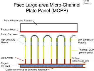
Micro-channel Plates PMTs Satisfies small feature size and homogeneity Photon and electron paths are short- few mm to microns=>fast, uniform Planar geometry=>scalable to large areas Fred Borcherding HEPD Visit
ANL Test-stand Measurements Jean-Francois Genat, Ed May, Eugene Yurtsev Sample both ends of transmission line with Photonis MCP (not optimum) 2picoseconds; 100 microns measured Fred Borcherding HEPD Visit
Simplifying MCP Construction Conventional Pb-glass MCP OLD Incom Glass Substrate NEW Chemically produced and treated Pb-glass does 3-functions: • Provide pores • Resistive layer supplies electric field in the pore • Pb-oxide layer provides secondary electron emission Separate the three functions: • Hard glass substrate provides pores; • Tuned Resistive Layer (ALD) provides current for electric field (possible NTC?); • Specific Emitting layer provides SEE Fred Borcherding HEPD Visit
Where we are with glass substrates .075” ~150 20m pores Hexagonal bundle of capillaries is called a `multi’. Each multi has ~15,000 capillaries Many many multis in an 8”-square plate. • Have received multiple samples of 10-micron, 20-micron, 40-micron glass substrates from Incom in 3/4”-sq and 33 mm round formats – will show results after ALD below • Two developments at Incom (our glass folks)- 1) 8” plates are being fabricated and the process improved, and 2) replacement of some multis with solid islands (`pads’) for installation of mechanical spacers. Idea is low cost amplification section - so far so good (hesitate to quote a # yet). INCOM glass substrate Incom, Inc Charlton, MA Fred Borcherding HEPD Visit
Sealed Tube (Tile) Construction • All (cheap) glass • Anode is silk-screened • No pins, penetrations • No internal connections • Anode determines locations (i.e. no mech tolerancing for position resolution) • Fastens with double-sticky to readout Tray: so can tile different length strings, areas • Tile Factory in works (ANL) Fred Borcherding HEPD Visit
The 24”x16” `SuperModule Fred Borcherding HEPD Visit
Glass Package Component Costs Rich Northrop Fabricated per unit cost estimates 30 1000 3000 10,000 100,000 Window (1@) $1813 11108 Side wall (1@) $7855524840 Base plate (1@) $201311108 Rod Spacers (75@) $7 32 1.20.80 Total $641 $306 $224 $158 $116 ---------Quotations--------- -----------------------Cost estimates---------------------- The above prices are for water jet cut B33 glass, tol. +- 0.010, except rod spacers +000 -0.004 Glass components are a small percentage of the proposed 8 x 8 MCP Fred Borcherding HEPD Visit
Atomic Layer Deposition (ALD) Thin Film Coating Technology • Atomic level thickness control • Deposit nearly any material • Precise coatings on 3-D objects (JE) • Lots of possible materials => much room for higher performance Jeff Elam pictures Fred Borcherding HEPD Visit
ALD for Emissive Coating Conventional MCP’s: Alternative ALD Coatings: (ALD SiO2 also) • Many material possibilities • Tune SEE along pore (HF- possible discrete dynode structure (speed!) Jeff Elam , Zeke Insepov, Slade Jokela Fred Borcherding HEPD Visit 23
MCP and Photocathode Testing Jeff Elam, Anil Mane, Qing Peng, Neal Sullivan (Arradiance), Bernhard Adams, Matt Wetstein, Slade Jokela, Igor Veryovkin, Alex Zinovev,, Ossy Siegmund SSL basic scrub period No Vacuum Bake • Conventional lead-oxide MCPs have single composition for resistive/emissive material • Functionalized in H-furnace requiring long “scrubbing” time (removal of volatiles) • ALD allows separate control of resistive and emissive layers • separately optimize each layer for best overall performance • Precise control over composition;tunable resistance • Arradiance coatings on Incom plate- Scrub time reduced by up to ×10 (!) (SSL) • Have functionalized several pairs with newly developed resistive layer plus Al2O3 secondary emissive layer (ANL) 40μm pore, L/D=40 MCPArradiance ALD coating image credit: J. McPhate ANL Signal from MCP pair coated with new resistive layer Al2O3 emissive layer image credit: M. Wetstein Large Area Photodetector Development Collaboration Fred Borcherding HEPD Visit 24
MCP and Photocathode Testing First measurements of gain in an ALD SEE layer at the APS laser test setup (Bernhard Adams, Matthieu Cholet, and Matt Wetstein) Testing Group: Bernhard Adams, Matthieu Cholet, and Matt Wetstein at the APS, Ossy Siegmund’s group at SSL N. B.! LAPPD Preliminary (very) Fred Borcherding HEPD Visit
First-ever test of an ALD pair (Ossy, SSL) Note- at high gain the boundaries of the multi’s go away Electron pattern (not a picture of the plate!)- SSL test, Incom substrate, Arradiance ALD. Note you can see the multi’s in both plates => ~50 micron resolution Fred Borcherding HEPD Visit
Simulation (crosses all groups)Valentin Ivanov, Zeke Insepov, Zeke Yusof, Sergey Antipov 10μm pore 40μm spacing Funnel (!) Large Area Photodetector Development Collaboration Fred Borcherding HEPD Visit 27
Photocathode Group Klaus Attenkofer, Zikri Yusof, Ossy Siegmund, Junqi Xi, Sasha Paramonov, Seon Wu Li, Slade Jokela, Ryan Dowdy (UIUC), Jim Buckley (WashU, Dan Leopold (WashU) • III-V have the potential for high QE, shifting toward the blue, and robustness i.e. they age well, high-temp) • Opaque PC’s have much higher QE than transmission PC’s- we have the geometry • Many small factors to be gained in absorption, anti-reflection- see papers by Townsend and talk by Fontaine on our web site • Quantum Effic. Of 50% have been achieved in multi-alkalis • Basic understanding is missing- we think we can make major contributions here to applications Big payoff if we can get >50% QE robust Photocathodes, and/or more robust (assembly). Also want to get away from `cooking recipes’ to rational design. Fred Borcherding HEPD Visit
SSL Photocathodes: Large Process Chamber – our backup (Ossy Siegmund) UV Transmissive Window Glass Window Manipulators 18” ID Chamber UHV valves Photo-Cathode Forming Well Flange 16.5” Detector Loading Flange Ion Pump supply Ion Pumps Fred Borcherding HEPD Visit 29
SSL Photocathodes: Processing Oven, Cathode Deposition • Oven accommodates Large Format Inside Envelope: 36” x 30” x 25” High • Defines Large Chamber Limits • Cathode station controls alkali metal deposition, and monitors cathode response Ossy Siegmund Fred Borcherding HEPD Visit • 30
Purchase of Burle PhotocathodeFacility (LDRD money) Fred Borcherding HEPD Visit
MCP/Photocathode Development- Test setup at APS laser Bernhard Adams, Klaus Attenkofer, (APS), Matt Wetstein (HEP), MatthieuChabon Fred Borcherding HEPD Visit
New Femtosec Laser Lab at APS • Bernhard Adams, Matthieu Chabon, Matt Wetstein Fred Borcherding HEPD Visit
Electronics GroupChicago- Hawaii • text Fred Borcherding HEPD Visit
Electronics GroupChicago- Hawaii Psec2 ASIC • 130nm IBM 8RF Process • This chip 4 channels, 256 deep analog ring buffer • Sampling tested at 11 GS/sec • Each channel has its own ADC- 9 bits eff (?) • The ADCs on this chip didn’t work due to leakage (silly, didn’t simulate slow easy things) - resubmitted, and test card out for fab with external ADC - will use 1 of 4 chnls • We’re learning from Breton, Delagnes, Ritt and Varner (Gary is of course a collaborator) Fred Borcherding HEPD Visit
Microstrip to Coplanar E-Field transition 36 Herve Grabas ? Simplest More complicated 0.15 millimeters 3.76 millimeters 50 Ohms 50 Ohms Many configurations are possible from very simple to complicated. Simulation and test can only tell which one will be the best. Fred Borcherding HEPD Visit
Summary • Glass substrates with ALD looks viable- still some questions and evolution, but looks good. • Basic questions on SSE materials are answered and are solid. • The necessary test and development facilities have been developed at SSL and ANL. • We have developed a `frugal’ 16”x24” design at ANL and a conservative but very solid 8”by 8” design at SSL; both places are close to making full-size proto-types • Multi-alkali photocathodes have been made at SSL and at Burle by ANL folks- we are much more confident than 6 months ago • We have attracted excellent young talent, less-young talent, interest from industry and applications- it’s a really good, highly-motivated group. Fred Borcherding HEPD Visit
Concerns • Funding- 4,3,1 vs 4, 2,2 • SuperModule design has led to larger area goal at 3-year end- goal now is enough SuperModules to engage industrial production (a step beyond `commercializable’)- Tile Factory wasn’t in the Proposal • We had requested strategic LDRD funds for the Photocathode Growth and Characterization Facility at ANL- just turned down (not unexpected)- • Missing an engineer/manager for the Tile Factory; photocathode effort still something of a pick-up ball game (but these can be the best, but a concern) Fred Borcherding HEPD Visit
THE ENDThanks to everybody in the LAPPD collaboration, esp. the young ones. Fred Borcherding HEPD Visit
Front-end Electronics/Readout Waveform sampling ASIC prototype • Varner, Ritt, DeLanges, and Breton have pioneered waveform–sampling onto an array of CMOS capacitors. Fred Borcherding HEPD Visit
SSL Tube Processing Facilities Sealed tube facilities and oven UHV detector/cathodeprocessing station
SSL Sealed tube detectorsPre-process assembly Planacon, with fiber optic window and cross strip anode (signal vias straight through substrate), in assembly with MCPsinstalled (above) ready to process.
SSL: Alkali Photocathodes • Jean-Francois Genat UCB SSL cathode compared with commercial product. Emissionspectrum of Cherenkov in water compared with bialkali response. Fred Borcherding HEPD Visit