Download
1 / 70
760 likes | 1.15k Vues
Noise Reduction Methods Intrinsic and Extrinsic. Rev 1.0. Contents. Intrinsic Noise Reduction Reduce Resistance, Bandwidth, or Amplifier Noise Averaging Extrinsic Noise Reduction PCB Layout Considerations Shielding Filtering Amplifier Rejection of RF Pick-up EMIRR.

E N D
Contents • Intrinsic Noise Reduction • Reduce Resistance, Bandwidth, or Amplifier Noise • Averaging • Extrinsic Noise Reduction • PCB Layout Considerations • Shielding • Filtering • Amplifier Rejection of RF Pick-up EMIRR
How to Reduce Noise • Select a low noise amplifier • Consider both current and voltage noise • Consider low and high frequency noise • Select the appropriate feedback resistors • Low Resistance for low noise • Limit the bandwidth
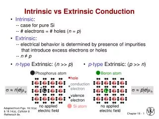
Voltage, Current, or Resistor Noise: Which dominates? Noise Current Analogous to IB MOS (fA/rtHz) Bipolar (pA/rtHz) Noise Voltage Analogous to VOS
What is the Spectral Density for Thermal Noise (from Resistors) Noise Spectral Density vs. Resistance en density = √ (4kTKR) Noise Spectral Density vs. Resistance nV/rt-Hz Resistance (Ohms)
Resistor vs. Amp Voltage Noise Resistor Noise Density Resistor enr> Op-Amp en 13nV/rtHz > 4.5nV/rtHz
Amp Current Noise vs. Amp Voltage Noise Voltage Noise env> Current Noise as Voltage eni 4.5nV/rtHz > 0.0025nV/rtHz
In the Data Sheet Low Frequency Noise on Scope Low Frequency Region 1/f Broadband Region
Adding noise sourcesTotal Noise Equation (Current or Voltage) enT = √[(en1/f)2 + (enBB)2] where: enT =Total rms Voltage Noise in volts rms en1/f = 1/f voltage noise in volts rms enBB = Broadband voltage noise in volts rms
where: fP = roll-off frequency of pole or poles fBF = equivalent brickwall filter frequency Real Filter Correction vs Brickwall Filter
AC Noise Bandwidth Ratios for nth Order Low-Pass Filters BWn = (fH)(Kn) Effective Noise Bandwidth Real Filter Correction vs Brickwall Filter
Broadband Noise Equation eBB BWn = (fH)(Kn) where: BWn = noise bandwidth for a given system fH = upper frequency of frequency range of operation Kn = “Brickwall” filter multiplier to include the “skirt” effects of a low pass filter enBB = (eBB)(√[BWn]) where: enBB = Broadband voltage noise in volts rms eBB = Broadband voltage noise density ; usually in nV/√Hz BWn = Noise bandwidth for a given system
en1/f = (e1/f@1Hz)(√[ln(fH/fL)]) where: en1/f = 1/f voltage noise in volts rms over frequency range of operation e1/f@1Hz = voltage noise density at 1Hz; (usually in nV) fH = upper frequency of frequency range of operation (Use BWn as an approximation for fH) fL = lower frequency of frequency range of operation e1/f@1Hz = (e1/f@f)(√[f]) where: e1/f@1Hz = normalized noise at 1Hz (usually in nV) e1/f@f = voltage noise density at f ; (usually in nV/√Hz) f = a frequency in the 1/f region where noise voltage density is known 1/f Noise Equation(see appendix for derivation) e1/f@1Hz
When does 1/f Noise Dominate Rule of Thumb: Broadband noise dominates if BW > 10 x ff
Simple Hand Calculation (is voltage or current noise dominant?)
Simple Hand Calculation (is voltage or current noise dominant?)
Simple Hand Calculation(Ignores current, resistor, and flicker noise)
Simulate To Check Vn-cal = 2.5mV rms Vn-sim = 2.77mV rms Reduce BW to reduce noise!
Reduce BW to 1kHz Vn-unfiltered = 2.77mV rms Vn-filtered = 0.2mV rms
Calculation Simulation Measurement
How to Reduce Noise • Select a low noise amplifier • Consider both current and voltage noise • Consider low and high frequency noise • Select the appropriate feedback resistors • Low Resistance for low noise • Limit the bandwidth
Links to Additional Reading Noise Article Series (www.en-genius.net) Tech-note Zone Operational Amplifier Noise: Techniques and Tips for Analyzing and Reducing Noise by Art Kay Published January 27, 2012 | ISBN-10: 0750685255
PCB Layout Considerations
Input Traces non-symmetrical: Common mode converted to differential
Output routed near sensitive analog (+) input: Positive Feedback
Basic PCB Design Principles • Separate Analog and Digital Signals • Pay Close Attention on Connecting AGND and DGND • Provide Good Ground Return Paths • High Frequency Bypassing • Minimize Inductance (Vital for HS) • Control Thermocouples • Fill void areas on signal layers with ground fill. • Taking care of these things will also help improve EMI/RFI performance.
Board Traces • Traces Can Act Like Antennas • Traces Have Transmission Line Properties • Inductance • Resistance • Traces for Power Should be Wide • Connect and Terminate Effectively (vias)
Source Signal Return Current Return Currents Digital Analog
Shielding for Noise Reduction
Skin Depth in Millimeters (mm) Absorption Loss = 9dB / skin depth
Shielding Effectiveness (S.E.) of enclosed material Emission Suppression S.EdB (Em. Supp.)≈ AdB Susceptibility S.EdB (Sus.) ≈ AdB + RdB (appropriate) where: A: absorption loss in dB R: reflection loss in dB From: COTS Journal, January 2004 – “Design Considerations In Building Shielded Enclosures.” Shielding and screening Minimizing the medium’s effectiveness Derived from: EDN – The Designer’s Guide to Electromagnetic Compatibility
Ferrite shield RF absorber shield Shielding and screening Minimizing medium’s effectiveness • Metal Shielding • Magnetic field f < 20kHz • Ferrous metals • steel • Mu-metal – nickel, iron • RF fields 10kHz < f < 1GHz • Non-ferrous metals • Al foil ILoss > 90dB • Cu, Ni ILoss 40-60dB • Vacuum plating • ILoss > 80dB • Electroless deposition • ILoss > 80dB • From: EDN EMI/EMC guide
Filtering for Noise Reduction
Input RC filtering as applied to an instrumentation amplifier Y Y X Capacitors X & 2Y Differential Mode f-3dB= 1/[2π(RA+ RB)(CA+ CB/2)] let RB = RA and CC = CB f-3dB= 343Hz Common Mode f-3dB= 1/[2π∙RA∙ CB)] let RB = RA and CC = CB f-3dB= 7.2kHz