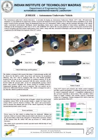
Download
1 / 43
430 likes | 567 Vues
Optoelectronic and Nonlinear Optical Processes. in Low Dimensiona Organic and Inorganic Semiconductors. Bhanu P. Singh Department Of Physics Indian Institute of Technology Bombay, Mumbai- 400076.

E N D
Optoelectronic and Nonlinear Optical Processes in Low Dimensiona Organic and Inorganic Semiconductors Bhanu P. Singh Department Of Physics Indian Institute of Technology Bombay, Mumbai- 400076
Nonliear optical systems, Nonlinearity & Its influence on opto - electronic response in low-d quantum confined systems Information Stress on Technology
Kerr slice with feedback mirror Theoretical model
Pattern generation in saturable absorber Thresholdintensity is given by where is given by following equation
Artificial design of complexity Nonlinear optical system to simulate 2-component reaction-diffusion system dynamics System with 2 Kerr slices and bounded feedback loops Variety of patterns
Some observed patterns Application to information processing
Quest for photonic materials Capacity for tailoring the optical properties such as (3) Eg-n and r -3 Property relationship with structure, interactions and ensuing processes Conjugated Polymers Semiconductors
PPV : optoelectronic material B.P.Singh et al,JNOPM,7,571(1998)
- LUMO R surface states PL emission + non-radiative transition primary absorption HOMO Surface states in semiconductor nanoparticles Quantum confined 0-d semiconductors Quantum dot transition probability spatial restriction Surface states provide highly efficient nonradiative channels and significantly quench the photoluminescence yield
Nanocomposites of CdS and ZnO EDAX and TEM - Approximately stoichiometric CdS and ZnO (Cd:S = 1:1.20 and Zn:O = 1:1.18)
SHUTTER PRESSURE GAUGE GAS FLOW LN2-COOLED SUBSTRATE HOLDER MAGNETRON GUN TURBO PUMP VIEW PORT SCRAPER RF magnetron sputtering - Experimental setup
Tunable source Detector Sample Linear absorption spectroscopy Itr= Iine-at
lexc Monochromator + PMT Comparative study of PL in CdS and CdS:ZnO nanocomposite films sample Vasa, Singh and Ayyub (in preparation)
Decay-time measurement Faster decay higher PL yield
lemi lexc film lexc = 458 nm Coherent PL from nanocomposite thin films Multiple beam interference observed in PL spectra Vasa, Singh and Ayyub (submitted) J. Phys. Cond. Mat
Ti:Sapphire Laser System 100 MHz, 800 nm, 80 fs BBO Lock-in Amplifier 400 nm Slit separation = 178 mm Slit width = 30 mm Sample-slit = 6.15 cm Slit-detector = 88.6 cm PMT slit width ~ 1 mm 121 Hz GG475 PMT Sample Double slit Double slit experiment - Setup
Experimental results Vasa, Singh and Ayyub J. Phys. Cond. Mat17,189(2005)
Lockin Tunablesource sample Powersupply Photocurrent spectroscopy Vasa, Singh, Taneja, Ayyub et. al, J. Phys. Cond. Mat, 14, 281 (2002)
IR Photocurrent spectroscopy Measurement against dark background Higher sensitivity Vasa, Singh and Ayyub (in preparation)
Pockels cell Ti:Sapphire Laser System 774 nm, 68 fs, 100 MHz 774 nm 68 fs, 3 Hz l/2 polarizer Data acquisition PD2 PD1 50% ARR Variable attenuator HR mirror sample R = 0.04 50% R = 0.04 ARINS - Experimental setup
CdS thin film (thickness = 1.3 mm) • Wavelength = 776 nm • Pulse width = 82 fs • Pulse rep. Rate = 3 Hz • Isample (max) ~ 0.8 GW/cm2 b = 48 cm/ GW b (CdS Single crystal) = 6.4 cm/GW at 780 nm
Dispersion of b for a CdS:ZnO nano-composite thin film b776nm (cm/GW) sample CdS (Single X´tl) 6.4 nano CdS 48 CdS:ZnO-2 129 • Presence of mid bandgap states • Free carrier absorption • Significant one photon, photo-current observed in IR Vasa, Singh and Ayyub (in preparation)
Quantitative measurement of One photon resonant nonlinearity Vasa, Singh and Ayyub (in preparation)
Ar+ oscilloscope Ti:Sapphire + BBO 391nm 100MHz detector chopper sample Carrier dynamics by pump-probe spectroscopy - Setup
Pump-probe spectroscopy - Results Carrier generation and relaxation time measurement
LUMO LUMO non radiative transition non radiative transition PL emission PL emission secondary absorption of PL or probe primary absorption of pump primary absorption of pump HOMO HOMO Origin of photo-darkening Free carrier absorption Excited state absorption Photo-induced chemical and/or structural changes
Solutions of rate equations LUMO N4 N3 fast non-radiative transition (~ps) secondary absorption of pump/PL/ probe (~ps) non-radiative transition (~10ps, gb) pl. emission (~100ps, ga) N2 primary absorption of pump (~ps, b) slow non-radiative transition (~2ms, gc) HOMO N1 Proposed 4-level model Vasa, Singh and Ayyub (in preparation)
Carrier generation and relaxation - data fitting
PL spectra as a function of incident intensity
Conclusions : • Self-organizing nonlinear optical system and information processing – enormous potential • Organic & inorganic low-d semiconductors – adaptable to property engineering • Constructive interference of one- and two-photon tributaries – must for large nonlinearity in organics by molecular engineering • Nonlinearity originating from exciton-phonon coupling – potential for NLO devices • Geometric ease in tailoring inorganic semiconductor quantum dots but organics have an edge • NLO processes may be detrimental to optoelectronic properties
Thank You Acknowledgement • TIFR • Parinda Vasa • Prof. P. Ayyub IITB • Prof. T. Kundu • A.V.V. Nampoothiri • Subal Sahani • Biswajit Pradhan • Binay Bhushan • Rajeev Sinha Department of Science and Technology