Overview of Control Hardware Development
380 likes | 537 Vues
Overview of Control Hardware Development.

Overview of Control Hardware Development
E N D
Presentation Transcript
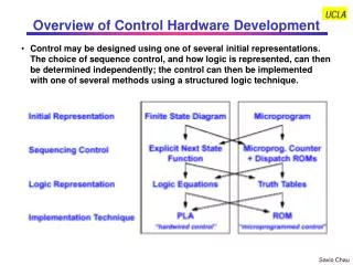
Overview of Control Hardware Development • Control may be designed using one of several initial representations. The choice of sequence control, and how logic is represented, can then be determined independently; the control can then be implemented with one of several methods using a structured logic technique.
Hardwired Control Approach • Simple to Implement See class example for drawing a finite state diagram for the multi-cycle add data path
0 0 0 X 0 0 1 add Example of State Transition and Control Signals Simple Multi-Cycle Data Path of add Instruction State # 0 (Instr Fetch) PC+4 PCwr = 1, IRwr = 1 RegWr = 0, ALUctr = X Next Address Logic PC Clk Control Unit Instruction Memory State # 1 (Decode/Operand Fetch) Opcode IRWr RegWr PCWr ALUctr 1 1 0 X PCwr = 0, IRwr = 0 RegWr = 0, ALUctr = X A Register File rs Rd addr1 rt ALU Rd addr2 Clk Instr Reg Wr addr rd B State # 2 (Exec & Write Back) Wr data Clk Clk PCwr = 0, IRwr = 0 RegWr = 1, ALUctr = add See class example for designing the simple state machine for the multi-cycle add data path
lw lw 1 0 0 0 1 0 0 0 0 0 1 0 0 1 X 1 X 0 X 1 X 0 0 1 0 1 0 0 X X X X X X X X 1 X 0 1 X X + X + X X + X X 1 0 X X 0 X add A Slightly More Complicate Example: Add & Lw State diagram Instruction Fetch #0 Decode/Operand Fetch #1 add #2 lw Add Exec Address Calculation #3 PC+4 Next Address Logic PC Mem Read & Write Back #4 Control Unit PCWr IRWr RegDst RegWr ExtOP ALUSrc ALUctr MemtoReg Instruction Memory Op Code Data Memory rs A Rd add1 rt Rd add2 ALU Instr Reg Reg File 0 ALU Out Reg mux Wr add rd 0 B 1 imm16 mux Wr data 1 ext 0 mux 1
1: PCWrite PCsrc = 10 x: others Initial Representation: Finite State Diagram 0 JComplete 9 J 8 2 1 3 5 6 10 11 7 4
Control Signals State N+1 Opcode 1 State N Sequencing Control: Explicit Next State Function State N+3 State N+2 State N+1 State N+2 See class examples for a simpler data path and control unit Next state number Current state number Each output line is a logical sum (i.e., OR) of minterms (i.e., AND) of the input lines. Example: NS3 = OP5·OP4·OP3·OP2·OP1·OP0·S3·S2·S1·S0 + OP5·OP4·OP3·OP2·OP1·OP0·S3·S2·S1·S0 + OP5·OP4·OP3·OP2·OP1·OP0·S3·S2·S1·S0 + S3·S2·S1·S0
Logic Representation: State Transition TableFor Next State Output Translating the State Diagram into State Transition Table See class example 2 for translating finite state diagram to state transition table
Logic Representation: Truth TableFor Next State Output Translating the State Transition Table into Truth Table See logic equation below Truth Table can be Translated into Logic Equations. Example: NS0 = S3·S2·S1·S0 + S3·S2·S1·S0·OP5·OP4·OP3·OP2·OP1·OP0 + S3·S2·S1·S0·OP5·OP4·OP2·OP1·OP0 + S3·S2·S1·S0 + + S3·S2·S1·S0
What About the Control Signals? PCsrc 2 1 0 MUX
1: PCWrite PCsrc = 10 x: others Control Signals and States 0 JComplete 9 J 8 2 1 3 5 6 10 11 7 4
Logic Representation: Logic EquationsFor Control Signal Output Translating the State Diagram into Control Output Table See class example 2 for translating finite state diagram to control output table
Logic Representation: Logic EquationsFor Control Signal Output For clarity, zeros are not shown in these columns See the simpler state machine in class example 2
Logic Representation: Logic EquationsFor Control Signal Output Truth Table of Output Signals: RegWrite = !S3 & S2 & !S1 & !S0 + !S3 & S2 & S1 & S0 + S3 & !S2 & S1 & S0
Example of Control Sequence: R-Type 0 0 0 0 0 0 0 1 0 0 0 0 0 0 1 0 0 0 0 1 0 0 0 0 0 0 1 0 0 0
Example of Control Sequence: R-Type 0 0 0 1 0 1 1 0 0 0 0 0 0 0 0 0 0 1 0 0 0 0 0 0 0 1 1 0 0 0
Example of Control Sequence: R-Type 0 1 1 0 0 1 1 1 0 0 0 0 0 0 0 0 0 0 0 0 0 0 0 1 0 0 0 1 0 0
Example of Control Sequence: R-Type 0 1 1 1 0 0 0 0 0 0 0 0 0 0 0 0 0 0 0 0 0 0 0 0 0 0 0 0 1 1
Example of Control Sequence: R-Type 0 0 0 0 0 0 0 1 0 0 0 0 0 0 1 0 0 0 0 1 0 0 0 0 0 0 1 0 0 0
AND Plane OR Plane IorD NS0 NS1 NS2 NS3 ExtOp IRWrite RegDst PCWrite ALUOp1 ALUOp0 ALUSrcA RegWrite MemWrite ALUSrcB1 ALUSrcB0 MemtoReg PCSource1 PCSource0 PCWriteCond OP5 OP4 OP3 OP2 OP1 OP0 S3 S2 S1 S0 Implementation Technique:Programmable Logic Array X 1 1 0 0 States that have mutliple next-states need multiple minterms
Programmable Logic Array Circuit Design AND Plane OR Plane Don’t care 0 1 1 selected on off 0 off on Don’t care 0 0 1 1 1 0
Summary of PLA Implemention of Multi Cycle Data Path Control Step 1: Develop the state diagram and assign a number to each state Step 2: Translate the state diagram into state transition table, in which each entry is consisted of the current state number and transition conditions (op code) as inputs, and the next state number and control signal as outputs Step 3: Translate the state transition table into truth table with all the bits shown explicitly Step 4: Translate the truth table into PLA diagram. Use the following convention in this class Step 5: Check the truth table and PLA diagram and make sure only one minterm is selected at any time (Note: some styles of PLA design allows multiple minterms selected, but it is more difficult because extreme care has to be used to make sure all output signals are correct in any state) Truth table entry 1 0 X 1 0 PLA representation Inputs (AND Plane) Outputs (OR Plane) Note: Step 1 is the most important. Many modern design tools have automated the other steps
Using Sequencer for Next State • For complex control functions, it is more efficient to use a sequencer to supply the sequential next state because the it requires less number of bits than encoding the next state explicitly
Sequencer-Based Control Unit AddrCtl For sequential state transitions, next state is automatically increased by the counter rather than explicitly supplied by the Next State output
Logic for Non-Sequential State Transitions AddrCtl AddrCtl Supplying an op code to the sequencer will force the finite state machine to the first state of the instruction
Implementing Control with a ROM • Since next-state address is supplied externally, a ROM can be used and needs only one word per state (“ Control word”). • In comparison, in the Explicit Next State Function approach, State 1 has 6 control words and State 2 has 2 control words. These are the same control signals as in the explicit next state discussion
Example: Micro Sequencer Operations for Load Bits 18 - 2 I Fetch Bits 1-0 Decode Adr Cal 0 Rd Mem Wr Reg 1 11 100011
Example: Micro Sequencer Operations for Load Bits 18 - 2 I Fetch Bits 1-0 Decode Adr Cal 1 Rd Mem Wr Reg 2 01 0011 0010 100011 100011
0011 0010 Example: Micro Sequencer Operations for lw Bits 18 - 2 I Fetch Bits 1-0 Bits 1-0 Decode Adr Cal 2 Rd Mem Wr Reg 3 10 0011 0010 100011 100011
Example: Micro Sequencer Operations for lw Bits 18 - 2 I Fetch Bits 1-0 Bits 1-0 Bits 1-0 Decode Adr Cal 3 Rd Mem Wr Reg 4 11 100011
Example: Micro Sequencer Operations for lw Bits 18 - 2 I Fetch Bits 1-0 Bits 1-0 Bits 1-0 Bits 1-0 Decode Adr Cal 4 Rd Mem Wr Reg 0 00 100011
Example: Micro Sequencer Operations for lw Bits 18 - 2 I Fetch Bits 1-0 Bits 1-0 Decode Adr Cal 0 Rd Mem Wr Reg 11 100011
Microprogram Implementation • ROM can be Thought of as a Sequence of Control Words • Control Word can be Thought of as an Instruction: “Microinstruction” • Rather Than Program in Binary, Use Symbolic Language Which Can Be Translated Into Input and Output Signals by a Microcode Assembler • Microprogramming: A Particular Strategy for Implementing the Control Unit of a Processor by “Programming” at the Level of Register Transfer Operations • MicroArchitecture: Logical Structure and Functional Capabilities of the Hardware as Seen by the Microprogrammer
ALU Control SRC1 SRC2 Reg Control Memory PC Write Control Sequencing Designing a Microinstruction Set • Start with List of Control Signals • Group Signals Together That Make Sense: Called “Fields” • Places Fields In Some Logical Order (ALU operation & ALU Operands First and MicroInstruction Sequencing Last) • Create a Symbolic Legend for the Microinstruction Format, Showing Name of Field Values and How They Set the Control Signals. Example: • To Minimize the Width, Encode Operations that Will Never be Used at the Same Time
MIPS Multicycle Microprogram for lw and sw Note: Usually it is safe to set all don’t cares to 0 or disabled
Two Styles of Microprogramming • Most Microprogramming- based Controllers Vary Between: • Horizontal Organization • 1 Control Bit Per Control Point • Vertical Organization • Grouping of Related Control Points into Encoded Fields • Need Additional Level of Decoding between the Control Word and the Actual Control Signals • Horizontal + More Control Over the Potential Parallelism of Operations in the Data-path - Uses up Lots of Control Store • Vertical + Compact Microinstruction Format + Easier to Program, Not Very Different from Programming a RISC Machine in Assembly Language - Extra Level of Decoding May Slow the Machine Down
Microprogramming Pros and Cons • Flexibility • Easy to Adapt to Changes in Organization, Timing, Technology • Can make Changes Late in Design Cycle, or Even in the Field • Can Implement Very Powerful Instruction Sets (just more control memory) • Generality • Can Implement Multiple Instruction Sets on Same Machine (Emulation) • Can Tailor Instruction Set to Application • Compatibility • Many Organizations, Same Instruction Set • Costly to Implement • Need sequencer and ROM (mostly external) • Slow • Need to read external ROM to get microinstructions • Microprogramming is suitable for processor designs on a circuit board, while PLA is suitable for processor designs on a chip