Advanced HPS Motherboard Design with Enhanced PCB Features
70 likes | 195 Vues
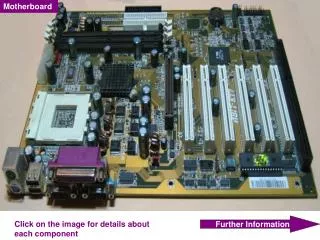
The HPS motherboard design incorporates a sophisticated electronic layout with 4 PCB layers, featuring 115 channels on the top left board. This design utilizes 115 AMP 10-pin SMD connectors for preamps and 15 TE signal connectors, maintaining compatibility with the previous version. Enhanced HV (15-pin DSUB) and LV (6-pin) connectors allow for improved routing. The layout adheres to strict specifications, including impedance control and ground ring placements. Key questions regarding preamp connection, pin positioning, thickness, and grounding practices are raised for clarification.

Advanced HPS Motherboard Design with Enhanced PCB Features
E N D
Presentation Transcript
HPS Motherboard Electronic Design • 4 PCB (115, 115, 106, 106 channels each). • For TOP LEFT board 115 channels we have: • 115 smd connectors (AMP 10 pin)for preamp very similar to previous version (pin slightly smaller). It is the same of FT-Cal motherboard.(next slide) • 15 TE signal connectors from 16 pin each, equal to previous version. (see page 3) • 2 HV connectors (15 pin) DSUB 750V, 5A, trough hole different to previous for a easier routing. • 1 LV connectors (6 pin). • We can use the same HV grouping. • We can use the same cable as discussed with Stepan Stepanyan.
HPS Motherboard Layout Design • For Layout design we have, probably, 10 layers. (3 signals + 1 for High Voltage + 1 fan-out + 5 GND). • Layout specifications: • 115 signal traces with 50 Ohms impedance. • Signal: 0.2 mm line width and 0.2 mm min. spacing. • HV: 0.6 mm line width and 0.9 mm min. spacing. • Ground ring between two signals as FT-Cal project.
Some Questions • 1)We assume preamp connection is the same of FT-Cal. Is it true? • 2)Preamp positioning. Where is located the HV pin respects yours picture? Last pin of right? Is the same for top and bottom part? • 3)Thickness between 3 or 4 mm for you. I think a 2.5 mm. Any problems? 4)Link the tin ground around the preamps holes to an internal ground layer with a via. Is it necessary? 5)You want put a tin ground without solder (circular area diameter 10mm) around each fixing hole. Why?