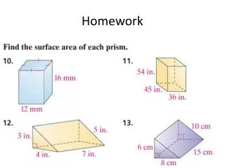
Homework
Homework. Reading Tokheim, Chapter 3, 4, and 6.1 - 6.3 Logg-o on Analytical Engine Website Machine Projects Continue on mp3 Labs Continue in labs with your assigned section. Digital Logic. Two types of digital logic design Combinational Logic – has no memory elements

Homework
E N D
Presentation Transcript
Homework • Reading • Tokheim, Chapter 3, 4, and 6.1 - 6.3 • Logg-o on Analytical Engine Website • Machine Projects • Continue on mp3 • Labs • Continue in labs with your assigned section
Digital Logic • Two types of digital logic design • Combinational Logic – has no memory elements • Sequential Logic – contains memory elements • Combinational logic design is sometimes called Boolean algebra after George Boole • Based on binary logic • Uses AND, OR, XOR, NOT, etc. • Develop truth tables and implement a design
Boolean Algebra • Variables / Expressions Two Values Only (0 or 1) • Basic Operators AND * OR + XOR + NOT Bar over the variable or expression Or # after variable name
Boolean Algebra • Precedence of Operators NOT (like unary minus) AND (like multiply) Division None OR/XOR (like add) Subtraction None • Parentheses to force precedence A * (B + C) is not the same as A * B + C
Boolean Algebra • Multiplicative Identities A * 0 = 0 A * A = A (Note: Not A squared) A * A = 0 • Additive Identities A + 1 = 1 A + A = A (Note: Not 2A) A + A = 1
Boolean Algebra • Negative Identity A = A • Commutative Property A * B = B * A A + B = B + A • Distributive Property A (B + C) = A * B + A * C
Boolean Algebra • Common Reductions of Sums of Products (Also called a “Minterm” expression) A * B + A * B + A * B = A + B OR A * B + A * B = A + B XOR • Common Reductions of Products of Sums (Also called a “Maxterm” expression) (A + B) * (A + B) * (A + B) = A * B AND
Basic Logic Gates • For a two input, one output gate, how many possibilities are there? • Assume a basic understanding of AND, OR, NOT, XOR and the negated forms: NAND and NOR x y ? z x y z 0 0 0 0 0 0 0 0 0 0 ... 1 0 1 0 0 0 0 1 1 1 1 ... 1 1 0 0 0 1 1 0 0 1 1 ... 1 1 1 0 1 0 1 0 1 0 1 ... 1
Binary Logic Symbols/Tables NOT AND 0 1 NAND 0 1 0 1 0 0 0 0 1 1 1 0 1 0 1 1 1 0
Binary Logic Symbols/Tables OR 0 1 0 1 XOR 0 1 NOR 0 0 1 0 1 0 0 0 1 1 1 1 1 0 0 1 1 0
Boolean Algebra / Logic Diagram • Sample Boolean Equation Y = (A + B) * (C + D) • Equivalent Logic Diagram A B Y C D
Basic Logic Gates • Can look at pulse trains over time as inputs rather than just constant inputs ???
Timing Considerations • Things don’t happen instantaneously • Each signal arrives at some unique time • Gate logic takes some time to react • Changes in the output appear some time after changes to the inputs (at nanosecond level) • Example, an AND gate A A Y B B Y
Timing Considerations • Things don’t happen instantaneously • As clock speed increases, the “skew” due to differential delays narrows output pulses • Beyond the designed maximum clock speed, the circuit may fail • Example, an AND gate A A Y B B Y
Practical Logic Implementation • Transistor-Transistor-Logic (TTL) Chips • Small Scale Integration (SSI) < 12 gates/chip • Medium Scale Integration (MSI) 12 - 99 gates/chip • 7400 series – Low Power Schottky (LS) • A good compromise between speed and power • Chips are generally 14- (or 16-pin) package • Vcc (+5 volts) usually on pin 14 (or pin 16) • Ground (0 volts) usually on pin 7 (or 8) • BUT NOT ALWAYS TRUE
Practical Logic Implementation • Logic Levels mapped to voltages in 2 ways: • Normal Logic Signal (name w/o a bar or #) • Logic 0 is < 0.8 volt • Logic 1 is > 2.0 volt • Inverted Logic Signal (name with a bar or #) • Logic 0 is > 2.0 volt • Logic 1 is < 0.8 volt