Download
1 / 16
160 likes | 270 Vues
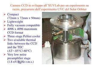
Camera CCD in sviluppo all’XUVLab per un esperimento su razzo, precursore dell’esperimento UVC del Solar Orbiter. Compact (72mm x 72mm x 50mm) Lightweight Fully vacuum compatible 4096 x 4096 maximum CCD format Three-stage Peltier cooler

E N D
Camera CCD in sviluppo all’XUVLab per un esperimento su razzo, precursore dell’esperimento UVC del Solar Orbiter • Compact(72mm x 72mm x 50mm) • Lightweight • Fully vacuum compatible • 4096 x 4096 maximum CCD format • Three-stage Peltier cooler • Two available thermal links between the CCD and the TEC (ΔT=-85°C/-60°C) • Very low noise preamplifier stage (1.8 nV/Hz r.m.s.)
Forme d’onda del CCD (fasi orizzontali in alto e verticali in basso) come appaiono ad uno strumento chiamato “analizzatore di stati logici”
Photomultipliers CCD Micro-Channel Plates Photodiodes (a-Si, treated Si, Al) Problemi dei rivelatori UV • high voltage, l > 110 nm, • low fluxes, dark current • low UV sensitivity, unstable, • not radiation hard, highly visible sensitive • high voltage, hygroscopic photocathodes, unstable gain, operated in UHV • low UV sensitivity, unstable, • not radiation hard, highly visible sensitive
radiation hardness visible blindness Requests very low noise chemical stability high sensitivity to XUV photons Ideal UV detector for space
Specifiche per i rivelatori del Solar Orbiter Common specification requirements for the imaging and spectroscopic instruments for remote sensing are • Solar blindness < 10-7 • Operating temperature ± 50°C • Frame rate 1000 s -1 • Frame format 2K 2K • Pixel size < 20 mm • Radiation hardness 50 Krad • Weight 1 kg Photon fluxes (counts/s/px) Imaging 103 Spectroscopy 102-103 3-D spectroscopy 105
Rivelatori UV disponibili Charge integration None! CCD is not rad-hard Photon Counting • MCP + XDL • MCP + APS • MCP + CID Advantages • Photon counting • Solar blindness • Radiation hardness • Spatialised • Operating @ Tamb Disadvantages • Efficiency < 30% • High voltage biases • Weight • Spatial resolution (centroid required) • External electronics (to be shielded!)
Alternativa: nuovi materiali fotosensibili Diamond & nitridesare appealing materials for the EUV photon detection. Their main properties are hereafter sumarized : • Eg = 5.5 eV dark current < 1 pA visible rejection (ratio 10-7) high EUV sensitivity • Highly radiation hard • Chemical inertness • Mechanically robust (high Young modulus) • High electric charge mobility = fast response time • Low dielectric constant = low capacitance
Rivelatori a diamante Device area: 6 6 mm2 Thickness: 40 µm Grain size: 20 µm Sensitive area 4 mm2 Interdigitated contacts spacing 20 m thickness 0.1 m electrode width 15 m No thermal annealing back contact 25 mm2
Toff = 30 % Stabilità e risposta temporale
Quantum Efficiency Diamond efficiency Comparisonwith other detectors [1] [2] [1] Naletto, Pace et al, 1994 [2] Wilhelm et al.,1995 E. Pace et al., Diam. Rel. Mater. 9 (2000) 987-993.
Diamond – Responsivity Dark current @ room temperature Vbias = 30 V
Our proposal: flip-chip CMOS imager • Select the most appropriate sensitive material • Exploit the advantages offered by the CMOS technology to fabricate system-on-a-chip detectors • Join the best material and on-chip CMOS electronics by means of the consolidated flip-chip technology (applied to IR photon and particle detection) The idea
Incident radiation Open electrode Sensitive layer CMOS imager 12.5 mm Pixel array Diamond bump-bonded detector
Applicazioni attuali alla fisica delle particelle
Advantages of flip-chip technology EUV sensitive layers bump-bonded on CMOS imagers could have many appealing features, such as: • High responsivity • Visible rejection • Available technologies • Frame format and pixel size in the spec • On-chip read-out electronics • Radiation hardness • Compact detector (reduced weight) • Low power consumption • High frame rate • Windowing