Homework
This resource explores the design and function of sequential circuits in digital logic, detailing components such as flip-flops, counters, and shift registers. It covers essential concepts, including the R-S flip-flop, D flip-flop operation, and the J-K flip-flop, along with applications like counting and data storage. The document also emphasizes the importance of clock signals in synchronous circuits, illustrating timing diagrams and truth tables to enhance understanding. Ideal for students and professionals working with digital electronics.

Homework
E N D
Presentation Transcript
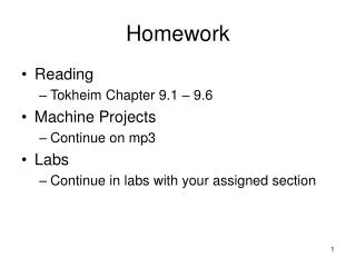
Homework • Reading • Tokheim Chapter 9.1 – 9.6 • Machine Projects • Continue on mp3 • Labs • Continue in labs with your assigned section
Sequential Circuits • A sequential circuit is constructed using a combinational circuit with memory circuits • Similar to a C function with static internal variables (state memory) • One additional input is a clock signal Input(s) Combinational Logic Output(s) Memory Elements Clock
Simple Memories (Flip-Flops) • Simplest is Reset-Set (R-S type) • Note the inverted signal inputs • Can buy a standard TTL R-S flip-flop (279) S Q S R Q Q 0 1 1 0 1 0 0 1 1 1 no change 0 0 prohibited Q R S NAND Q NAND Q R
Simple Memories (Flip-Flops) No Effect • Timing Diagram S R Q Q No Effect Hold Set Hold Reset Hold Hold 1 0 1 0 1 0 1 0
Synchronous Flip-Flops • Use of a clock to make the circuit synchronous • Syn (with) + chronous (clock) => with a clock • Level-triggered (changes state while clock high) S S TRUTH TABLE S R Clock Q 0 1 0 1 0 1 0 0 No Chg 1 1 Prohibited NAND R-S Flip Flop Q Clock NAND Q R R
The D-Type Flip-Flop • Single data input and edge-triggered clock • Also called a “Delay” flip-flop (D-type) • Changes state on either rising or falling edge D (Data) S TRUTH TABLE D Clock Q 0 0 1 1 NAND R-S Flip Flop Q NAND Q R C Clock A • Edge To Pulse Converter • A B C • 0 1 0 • 1 1 (Due to delay through inverter) • 1 0 0 AND B
Actual D-Type Flip-Flop • Has preset (PR) and clear (CLR) inputs which can be set asynchronously (but not both at same time) • Nomenclature use > for an edge-triggered input PR D Q > Clk Q CLR
Clock - Divide by Two Counter • Connect Q output back to D input • Timing Diagram (after starting with Q = 0) PR D Q > Clk Q CLR Clk Q Q is an output clock at ½ the frequency of the input clock
Shift Registers • Serial in, Parallel out: Four Bit Parallel Output Available After Four Clocks/Shifts Serial Data In D Q D Q D Q D Q FF1 FF1 FF1 FF1 Clock In
Shift Registers • Parallel in, Serial out: Four Bit Parallel Input Presented for One Clock Edge while “Load” Signal is True Load/Shift# M U x M U x M U x M U x Serial Data Out 1 D Q D Q D Q D Q FF1 FF1 FF1 FF1 Clock In
The J-K or Universal Flip-Flop • Named for Jack Kilby (TI Engineer / Inventor of IC) • Three synchronous inputs (plus preset and clear) • J-K flip-flop is available as a 7473 chip • Can be edge-triggered or level-triggered • Example shown is falling “edge triggered” TRUTH TABLE J K Clock Q 0 0 Stays same 0 1 0 1 0 1 1 1 Toggles PR J Q >Clk K Q CLR
J-K Flip-Flop Internals • Avoids an invalid input such as 0 0 to the R-S Flip Flop AND S K R-S Flip Flop Q Edge Detect Clock AND Q J R
Using J-K Flip-Flops • Primary use is for storage registers and counters • Mod-16 counter also known as a ripple counter X3 X2 X1 X0 counts 0x0 ... 0xF (Hexadecimal) sequentially X1 X2 X3 X0 J Q J Q J Q J Q Clk > > > > K K K K Vcc (+5 V)
Timing diagram for Mod-16 Counter Note that the counter actually serves to divide down the input clock!
Counter Range != 2N X0 X1 X2 NAND Vcc (+5 V) J Q J Q J Q > > > K K K Reset Clk • Can we we make it count to something different than 2N? • Ans. Yes, using a combinational logic (a NAND Gate in this case) • Counts: 0, 1, 2, 3, 4, 5, 0, 1, …
Synchronous BCD up/down counter • BCD Up/Down Counter is available as a 74192 • BCD stands for Binary Coded Decimal • Counts 0000 -1001, then carries LED Bit Display D QD C QC B QB 74192 BCD Up/Down Counter A QA Load Data Borrow Count Up Count Down Clear Carry
Describing Sequential Circuits • In general, • Next state = f(inputs, current state) • Outputs = f(inputs, current state) • Example: • State diagram:
Digital Logic Summary • Combinational circuits: • Made from gates without feedback • Have no internal states • Outputs depend only on current inputs • Fully defined by truth table on the inputs • Passes clocks (if any) as wave trains • Output states constantly change with inputs
Digital Logic Summary • Sequential circuits: • Have feedback among the gates • Can have internal states • Outputs depend on inputs and past inputs (via values of internal states) • Not completely described by pure truth table on inputs • Usually one input is a clock signal • Outputs usually change on one clock edge only