Download
1 / 1
30 likes | 217 Vues
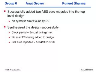
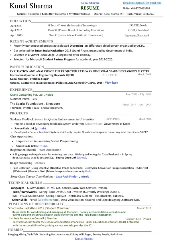
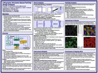
Device Analyses. a. b. < -8nm. -7nm, -6nm. -5nm, -4nm. -3nm, -2nm. +2nm, -3nm. Experiments & Results. +4nm, +5nm. +6nm, +7nm. SPICE Netlists. Library. Characterize. For LVS. Objective. Std. Cell GDS. Device Analyses. Objective-Specific Verilog. Drawn Layout (DEF).

E N D
Device Analyses a b < -8nm -7nm, -6nm -5nm, -4nm -3nm, -2nm +2nm, -3nm Experiments & Results +4nm, +5nm +6nm, +7nm SPICE Netlists Library Characterize For LVS Objective Std. Cell GDS Device Analyses Objective-Specific Verilog Drawn Layout (DEF) Lithosimulated Layout (GDS) Interconnect Analysis Update Parasitics (SPEF) Delay, Power, etc. Analyses Interconnect Analyses Full-Chip Analyses Lithography Simulation-Based Full-Chip Design AnalysesPresenter: Puneet Sharma (sharma@ucsd.edu) • Average Gate-width (WAvg) computation • Diffusion boundary may not be straight match diffusion area in dotted rectangle (a, b > misalignment tolerance) • Average width = separation b/w computed diffusion boundaries • Average Gate-length (LAvg) computation • Take intersection b/w diffusion and poly get gate • Gate not rectangular rectilinearize (midpoint-sum approx.) • LAvg computed from gate-lengths of slices after rectilinearization Specific to analysis objective. Two modes: • Expression mode: computed using analytical expressions • e.g., for delay objective: LAvg = WAvg/Σi(Wi/Li) • for capacitance objective: LAvg = Σi(WiLi)/WAvg • Lookup-table mode: computed using table of device on- and off- currents for different gate-lengths and gate-widths • Mapping to a cell in library • Each cell instance prints different uniquification of each instance need to reconstruct hierarchy • Equivalent gate-length (LEq) computation: derived from LAvg’s of devices in the cell. Specific to analysis objective. LEq for objective: • setup is max. of LAvg’s. • hold is min. of LAvg’s. • capacitance is computed to match the gate area • leakage is computed to match the total leakage can consider stacking effect to weigh devices differently • For each cell, variant from library selected that has closest gate-length to LEq of cell, and master updated in output Verilog • Invokes device analyses per instance and interconnect analyses for SPEF database • Can perform caching and distributed processing • Mixed-mode objective • Separate Verilogs generated for different objectives difficult to manage and non-standard mixed-mode objective generates one Verilog accurate for all objectives as follows: • Step 1: hold objective for hold-critical cells • Step 2: setup objective for setup-critical cells • Step 3: capacitance objective for fanout cells of hold and setup critical cells not assigned objective • Step 4: leakage/dynamic power for all other cells Effective Diffusion Area Simulated Diffusion Contour P. Gupta†, A. B. Kahng†‡, S. Nakagawa†, S. ShahΨ, P. Sharma‡ †Blaze DFM Inc., Sunnyvale, CA ‡ECE Department, U.C. San Diego ΨEECS Department, U. of Michigan Drawn Diffusion Boundary Computed Diffusion Boundary Drawn Poly Motivation • Timing and power sign-off before RET • Similarity b/w drawn and printed design poor due to RETs and process variations • Large difference b/w signed-off and on-silicon power & delay • Lithography simulation predicts on-silicon geometries at different process corners • However, lithography simulation purely geometry-based and not connected to design in any way • We use lithography simulation w/ off-the-shelf design analysis tools to predict on-silicon performance & power • Facilitates more accurate estimation lesser guardbanding • Previous work: Yang et al. DAC 05 – similar flow suggested; several non-trivial details lacking; timing analysis only (for critical paths); no interconnects considered Layout of a small circuit litho-simulated at 0nm and 200nm defocus Analyses for setup and leakage objectives; color annotations show LEq Practical runtime: 70K cell design in 1hr Midpoint-sum approximation Rectilinearize Setup, Defocus = 0nm Setup, Defocus = 200nm Overview Cycle time 0.351ns Cycle time 0.363ns • Inputs: • Litho-simulated GDS • Drawn layout: to correlate GDS with design • Std. cell GDS and SPICE netlists: to run LVS find location of each device in a cell layout • Std. cell library w/ gate-length changed for devices in cells • Objective: type of analysis to be performed e.g., setup time, hold time, leakage, dynamic power • Outputs: • Objective-specific Verilog: Verilog with cell masters modified to better estimate on-silicon power/performance • SPEF: modified parasitics • Device Analyses: For each cell, analyzes litho-simulated poly layer to estimate gate-length of cell’s devices searches library for similar cell with non-nominal gate-lengths (cell variant) modifies master in Verilog • Interconnect Analyses: For each interconnect, analyzes impact of non-ideal geometry on parasitics updates SPEF Leakage, Defocus = 0nm Leakage, Defocus = 200nm Leakage 1.488mW Leakage 2.789mW Conclusions & Ongoing Work Parasitic-change lookup table: predicts change in capacitance and resistance given change in interconnect width and spacing Parameters: width, width and spacing of right and left neighbors, layer, densities of above and below layers Table created by field-solver simulations for geometries generated for a technology Lithography simulation-based parasitic extraction SPEF segment to routing segment mapping: for each routing segment in SPEF, corresponding geometries in drawn and litho-simulated layouts are found using SPEF node coordinates Shape rectilinearization: litho-simulated routing segments not rectilinear perform rectilinearization similar to gate-poly SPEF database modification: parasitic change computed from lookup table for each slice (from rectilinearization) parasitic network reduction update SPEF database • Lithography simulation not connected to design we proposed a novel flow to link lithography simulation w/ off-the-shelf analyses tools • For device analyses, device rectilinearized and LAvg computed. Devices in each cell considered to find LEq of cell and closest library variant used • For interconnect analyses, impact of change in dimension on capacitance and resistance estimated using field-solver for template configurations and SPEF database modified • Lithography simulation-based analyses more accurate and adequately fast • Ongoing work: • Consider impact of slice location on LAvg computation • Transistor-level delay and power modeling to replace or supplement library chacterization • Improve speed and accuracy of interconnect analyses