1 / 22
220 likes | 350 Vues
calculation of quantum conductance for resonant tunneling

E N D
Course: Quantum Electronics Arpan Deyasi Quantum Topic: Resonant Tunneling Electronics Arpan Deyasi Arpan Deyasi, RCCIIT, India 5/6/2021 1
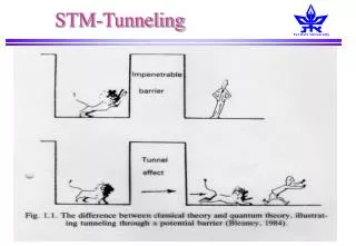
Resonant tunneling at unbiased condition Arpan Deyasi Quantum Electronics Barrier 5/6/2021 Arpan Deyasi, RCCIIT, India 2
Resonant tunneling at unbiased condition Arpan Deyasi Quantum Electronics 5/6/2021 Arpan Deyasi, RCCIIT, India 3
Mathematical Formulation Arpan Deyasi 2 2 d − + = V E Under unbiased condition Quantum * 2 2 m dz If electric field ‘ξ’ is applied Electronics 2 2 d ( ) − + − q z = V E * 2 2 m dz 5/6/2021 Arpan Deyasi, RCCIIT, India 4
Resonant tunneling at biased condition Arpan Deyasi Quantum misalignment Electronics ξ1 5/6/2021 Arpan Deyasi, RCCIIT, India 5
Resonant tunneling at biased condition Arpan Deyasi Quantum Electronics ξ2> ξ1 5/6/2021 Arpan Deyasi, RCCIIT, India 6
Condition for Resonant Tunneling Consider double quantum well system under application of electric field Arpan Deyasi Assume thickness of middle barrier is such that resonant tunneling occurs between adjacent quantum wells Quantum Current due to electrons flowing from left-to-right Electronics d q f E = ( ), 2 ( ) ( )2 I v T L L 0 5/6/2021 Arpan Deyasi, RCCIIT, India 7
Condition for Resonant Tunneling T(κ): transmission probability Arpan Deyasi v(κ): velocity of electron wave when energy levels of adjacent quantum wells are matched Quantum μ(L): Fermi level of left quantum well Electronics f: Fermi function 5/6/2021 Arpan Deyasi, RCCIIT, India 8
Condition for Resonant Tunneling From parabolic dispersion relation Arpan Deyasi Quantum 2 2 = E Electronics * 2 m dE d= 2 dE d = v * m 5/6/2021 Arpan Deyasi, RCCIIT, India 9
Condition for Resonant Tunneling Equation of current becomes Arpan Deyasi Quantum dE q f E = Electronics ( ), 2 ( ) ( )2 I v E T E L L ( ) v E 0 dE q f E = ( ), ( ) T E I L L 0 5/6/2021 Arpan Deyasi, RCCIIT, India 10
Condition for Resonant Tunneling Arpan Deyasi dE h = ( ), I Quantum 2 ( ) T E q f E L L U L UL: lower limit of Fermi function at left side Electronics 5/6/2021 Arpan Deyasi, RCCIIT, India 11
Condition for Resonant Tunneling Current due to electrons flowing from right-to-left Arpan Deyasi R Quantum dE h = ( ), 2 ( ) T E I q f E R Electronics U R UR: lower limit of Fermi function at right side 5/6/2021 Arpan Deyasi, RCCIIT, India 12
Condition for Resonant Tunneling Net current (assuming flowing from left-to-right) Arpan Deyasi L Quantum = − I I I net R Electronics 2 q h ( ) = ( ), − ( ), ( ) T E dE f E f E L R U L Resonant tunneling equation from Esaki and Tsu 5/6/2021 Arpan Deyasi, RCCIIT, India 13
Calculation of Conductance For constant applied bias, device is operated at lower temperature Arpan Deyasi electrons become highly degenerate Quantum Make applied bias very low Electronics Fermi function can be expanded in Taylor series form 5/6/2021 Arpan Deyasi, RCCIIT, India 14
Calculation of Conductance ( ), Arpan Deyasi − ( ), f E f E Quantum L R 1 2 1 2 Electronics + − − , , f E qV f E qV 5/6/2021 Arpan Deyasi, RCCIIT, India 15
Calculation of Conductance Arpan Deyasi 1 2 1 2 ( , ) f E = + + ( ) f E Quantum qV ( , ) f E ( ) f E Electronics − − − qV ( , ) f E = qV 5/6/2021 Arpan Deyasi, RCCIIT, India 16
Calculation of Conductance Substituting in the expression of Esaki and Tsu Arpan Deyasi Quantum 2 ( , ) f E q h = ( ) T E dE I qV net Electronics U L 2 2 ( , ) f E q V h = ( ) T E dE I net U L 5/6/2021 Arpan Deyasi, RCCIIT, India 17
Calculation of Conductance Arpan Deyasi Conductance Quantum 2 ( , ) f E I q h = = 2 ( ) T E dE G net V Electronics U L 5/6/2021 Arpan Deyasi, RCCIIT, India 18
Quantum unit of Conductance The term (q2/h) is called quantum unit of conductance Arpan Deyasi Quantum Q.U.C = 38.7 μS Corresponding resistance = 25.8 KΩ Electronics 5/6/2021 Arpan Deyasi, RCCIIT, India 19
Calculation of Conductance If temperature is very low Arpan Deyasi Quantum ( , ) f E → ( ) E Electronics 5/6/2021 Arpan Deyasi, RCCIIT, India 20
Calculation of Conductance Arpan Deyasi 2 q h G Quantum = ( ) ( ) E T E dE 2 U L Electronics 2 q h = 2 ( ) T E G 5/6/2021 Arpan Deyasi, RCCIIT, India 21
Calculation of Conductance ( ) T E → Arpan Deyasi 1 If Corresponding resistance = 12.9 KΩ Quantum Electronics 5/6/2021 Arpan Deyasi, RCCIIT, India 22