Download
1 / 5
50 likes | 240 Vues
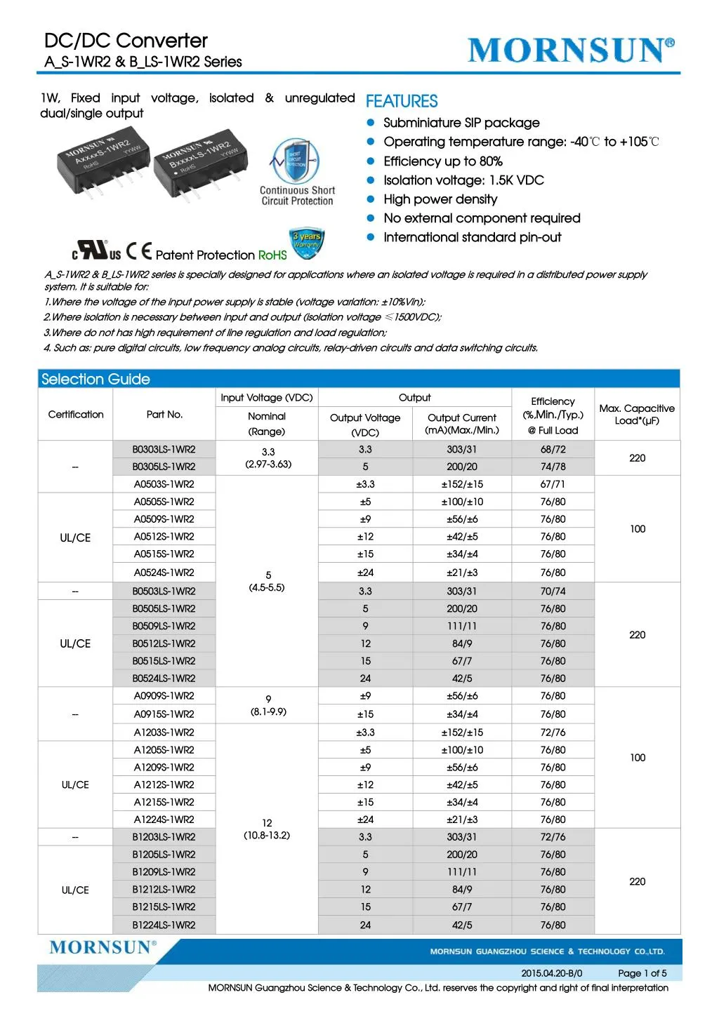
A_S-1WR2 & B_LS-1WR2 series is specially designed for applications where an isolated voltage is required in a distributed power supply<br>system. It is suitable for:<br>1.Where the voltage of the input power supply is stable (voltage variation: ±10%Vin);<br>2.Where isolation is necessary between input and output (isolation voltage ≤1500VDC);<br>3.Where do not has high requirement of line regulation and load regulation;<br>4. Such as: pure digital circuits, low frequency analog circuits, relay-driven circuits and data switching circuits

E N D
DC/DC Converter A_S-1WR2 & B_LS-1WR2 Series FEATURES ? Subminiature SIP package ? Operating temperature range: -40℃ to +105℃ ? Efficiency up to 80% ? Isolation voltage: 1.5K VDC ? High power density ? No external component required ? International standard pin-out 1W, dual/single output Fixed input voltage, isolated & unregulated Patent Protection RoHS A_S-1WR2 & B_LS-1WR2 series is specially designed for applications where an isolated voltage is required in a distributed power supply system. It is suitable for: 1.Where the voltage of the input power supply is stable (voltage variation: ±10%Vin); 2.Where isolation is necessary between input and output (isolation voltage ≤1500VDC); 3.Where do not has high requirement of line regulation and load regulation; 4. Such as: pure digital circuits, low frequency analog circuits, relay-driven circuits and data switching circuits. Selection Guide Input Voltage (VDC) Output Efficiency (%,Min./Typ.) @ Full Load Max. Capacitive Load*(μF) Certification Part No. Nominal (Range) Output Voltage (VDC) 3.3 Output Current (mA)(Max./Min.) B0303LS-1WR2 303/31 68/72 3.3 220 (2.97-3.63) B0305LS-1WR2 5 200/20 74/78 -- A0503S-1WR2 ±3.3 ±152/±15 67/71 A0505S-1WR2 ±5 ±100/±10 76/80 A0509S-1WR2 ±9 ±56/±6 76/80 100 A0512S-1WR2 ±12 ±42/±5 76/80 UL/CE A0515S-1WR2 ±15 ±34/±4 76/80 A0524S-1WR2 ±24 ±21/±3 76/80 5 (4.5-5.5) -- B0503LS-1WR2 3.3 303/31 70/74 B0505LS-1WR2 5 200/20 76/80 B0509LS-1WR2 9 111/11 76/80 220 UL/CE B0512LS-1WR2 12 84/9 76/80 B0515LS-1WR2 15 67/7 76/80 B0524LS-1WR2 24 42/5 76/80 A0909S-1WR2 ±9 ±56/±6 76/80 9 (8.1-9.9) -- A0915S-1WR2 ±15 ±34/±4 76/80 A1203S-1WR2 ±3.3 ±152/±15 72/76 A1205S-1WR2 ±5 ±100/±10 76/80 100 A1209S-1WR2 ±9 ±56/±6 76/80 UL/CE A1212S-1WR2 ±12 ±42/±5 76/80 A1215S-1WR2 ±15 ±34/±4 76/80 A1224S-1WR2 ±24 ±21/±3 76/80 12 (10.8-13.2) -- B1203LS-1WR2 3.3 303/31 72/76 B1205LS-1WR2 5 200/20 76/80 B1209LS-1WR2 9 111/11 76/80 220 B1212LS-1WR2 12 84/9 76/80 UL/CE B1215LS-1WR2 15 67/7 76/80 B1224LS-1WR2 24 42/5 76/80 Page 1 of 5 2015.04.20-B/0 MORNSUN Guangzhou Science & Technology Co., Ltd. reserves the copyright and right of final interpretation
DC/DC Converter A_S-1WR2 & B_LS-1WR2 Series A1505S-1WR2 A1512S-1WR2 A1515S-1WR2 B1505LS-1WR2 B1512LS-1WR2 B1515LS-1WR2 A2405S-1WR2 ±5 ±12 ±15 5 12 15 ±5 ±100/±10 ±42/±5 ±34/±4 200/20 84/9 67/7 ±100/±10 76/80 76/80 76/80 76/80 76/80 76/80 76/80 -- 100 15 (13.5-16.5) CE -- CE 220 A2409S-1WR2 ±9 ±56/±6 76/80 UL/CE A2412S-1WR2 ±12 ±42/±5 76/80 100 A2415S-1WR2 ±15 ±34/±4 76/80 A2424S-1WR2 ±24 ±21/±3 76/80 24 -- B2403LS-1WR2 3.3 303/31 70/74 (21.6-26.4) B2405LS-1WR2 5 200/20 76/80 B2409LS-1WR2 9 111/11 76/80 220 UL/CE B2412LS-1WR2 12 84/9 76/80 B2415LS-1WR2 15 67/7 76/80 B2424LS-1WR2 24 42/5 76/80 Note:*The capacitive loads of positive and negative outputs are identical. Input Specifications Item Operating Conditions Min. Typ. Max. Unit 3.3V input -- 426/30 --/70 5V input -- 281/25 --/60 9V input -- 142/20 --/60 Input Current (full load / no-load) mA 12V input -- 106/15 --/50 15V input -- 84/10 --/35 24V input -- 54/7 --/30 3.3V input -0.7 -0.7 -- -- 5 9 5V input 9V input -0.7 -0.7 -- -- 12 18 Surge Voltage (1sec. max.) VDC 12V input 15V input -0.7 -- 21 24V input -0.7 -- 30 Reflected Ripple Current -- 15 Capacitor filter -- mA Input Filter Hot Plug Unavailable Output Specifications Item Operating Conditions Min. Typ. Max. Unit Output Voltage Accuracy See tolerance envelope graph (Fig. 1) 3.3VDC output -- -- ±1.5 Input voltage change: ±1% Line Regulation -- Other output -- -- ±1.2 3.3VDC output -- -- 18 % 5VDC output -- -- 12 Load Regulation 10%-100% load 9VDC output 12VDC output -- -- 9 -- -- 8 % 15VDC output -- -- 7 Load Regulation 10%-100% load 24VDC output -- -- 6 Ripple & Noise* 20MHz bandwidth -- 60 150 mVp-p Temperature Drift Coefficient 100% load -- -- ±0.03 %/℃ Page 2 of 5 2015.04.20-B/0 MORNSUN Guangzhou Science & Technology Co., Ltd. reserves the copyright and right of final interpretation
DC/DC Converter A_S-1WR2 & B_LS-1WR2 Series A24xxS-1WR2 /B24xxLS-1WR2 A0524S-1WR2/B0524LS-1WR2 others -- -- 1 s Output Short Circuit Protection** Continuous, self-recovery Note: * Ripple and noise tested with “parallel cable” method, please see DC-DC Converter Application Notes for specific operation methods. **Supply voltage must be discontinued at the end of short circuit duration for A24xxS-1WR2 /B24xxLS-1WR2 series, and A0524S-1WR2/ B0524LS-1WR2 models. General Specifications Item Operating Conditions Input-output, with the test time of 1 minute and the leak current lower than 1mA Input-output, insulation voltage 500VDC Input-output, 100KHz/0.1V Derating if the temperature ≥85°C, (see Fig. 2) Min. Typ. Max. Unit Insulation Voltage VDC 1500 -- -- Insulation Resistance Isolation Capacitance Operating Temperature Storage Temperature Casing Temperature Rise Pin Welding Resistance Temperature Storage Humidity Switching Frequency MTBF MΩ pF 1000 -- -40 -55 -- -- -- -- 3500 -- 20 -- -- 25 -- -- 100 -- -- -- 105 125 -- 300 95 -- -- ℃ Ta=25℃ Welding spot is 1.5mm away from the casing, 10 seconds Non-condensing 100% load, nominal input voltage MIL-HDFK-217F@25℃ %RH KHz K hours Physical Specifications Casing Material Black flame-retardant heat-proof epoxy resin (UL94-V0) Package Dimensions 19.50*9.30*6.00 mm Weight 2.4g(Typ.) Cooling methods Free air convection EMC Specifications Conducted disturbance Radiated emission CISPR22/EN55022 CISPR22/EN55022 IEC/EN61000-4-2 IEC/EN61000-4-2 CLASS B (see Fig. 4 for recommended circuit) CLASS B (see Fig. 4 for recommended circuit) Contact ±6KV perf. Criteria B Contact ±8KV perf. Criteria B EMI A_S-1WR2 B_LS-1WR2 EMS Electrostatic discharge Product Characteristic Curve 3.3VDC output Tolerance Envelope Curve Other output Tolerance Envelope Curve (%) Accuracy +15% +10% (%) Accuracy Max. +10% +5% Max. +1.0% +5% 0 Typ. Typ. Output Voltage +2.5% Output Voltage 0 -5% Min. -2.5% -7.5% -5% Min. -10% -7.5% -10% -15% -15% 10% 20% 40% 80% 100% 60% 10% 20% Output Current Percentage(%) (Nominal Input Voltage) 40% 80% 100% 60% Output Current Percent(%) (Nominal Input Voltage) Fig. 1 Page 3 of 5 2015.04.20-B/0 MORNSUN Guangzhou Science & Technology Co., Ltd. reserves the copyright and right of final interpretation
DC/DC Converter A_S-1WR2 & B_LS-1WR2 Series Temperature Derating Curve Output Power Percent(%) 120 100 80 60 Safe Operating Area 40 20 0 105 40 85 0 -40 Ambient Temp.( Fig. 2 ) ℃ Efficiency Vs Input Voltage (Full load) Efficiency Vs Output Load(Vin=5V) 100 100 95 90 90 80 A0505S-1WR2 Efficiency(%) 85 70 Efficiency(%) A0505S-1WR2 80 60 75 50 70 40 65 30 60 20 55 10 50 0 4.5 4.6 4.7 4.8 4.9 5.0 5.1 5.2 5.3 5.4 5.5 Input Voltage (V) Efficiency Vs Input Voltage (Full Load) 10 20 30 40 50 60 70 80 90 100 Output Current Percentage (%) Efficiency Vs Output Load(Vin=24V) 100 100 95 90 90 A2415S-1WR2 80 85 70 Efficiency(%) Efficiency(%) A2415S-1WR2 80 60 75 50 70 40 65 30 60 20 55 10 50 0 21.622.0 22.5 23.0 23.5 24.0 24.5 25.0 25.5 26.0 26.4 Input Voltage (V) 10 20 30 40 50 60 70 80 90 100 Output Current Percentage (%) Design Reference 1. Typical application If it is required to further reduce input and output ripple, a filter capacitor can be connected to the input and output terminals, see Fig.3. Moreover, choosing suitable filter capacitor is very important, start-up problems may be caused by too large capacitance. To ensured the modules running well, the recommended capacitive load values as shown in Table 1. Recommended capacitive load value table (Table 1) Vin (VDC) (μF) (VDC) 3.3/5 4.7 3.3/5 Dual Cin Single Vout Cout (μF) 10 Dual Vout (VDC) ±3.3/±5 Cout (μF) 4.7 +Vo Vin Cout DC 0V DC Cin Cout GND -Vo 9/12 15 24 2.2 2.2 1 9/12 15/24 -- 2.2 1 -- ±9/±12 ±15/±24 -- 1 Single 0.47 -- +Vo Vin DC DC Cout Cin GND 0V It is not recommended to connect any external capacitor when output power is less than 0.5W. Fig.3 Page 4 of 5 2015.04.20-B/0 MORNSUN Guangzhou Science & Technology Co., Ltd. reserves the copyright and right of final interpretation
DC/DC Converter A_S-1WR2 & B_LS-1WR2 Series 2. EMC typical recommended circuit (CLASS B) LDM Vin Input voltage (VDC) 3.3/5/9/12 15/24 Vin +Vo C1 C2 CY LDM 4.7μF /50V DC/DC LOAD C1 C2 Refer to the Cout in Fig.3 -- 6.8μH EMI 1nF/2KV -Vo (0V) GND GND CY Note: 1.15V/ 24V input series is subject to CY (CY : 1nF/2KV). 2. It is not needed to add the component in the peripheral circuit when parameter with the symbol of "--". Fig. 4 3. Output load requirements To ensure the module work efficiently and reliably, during the operation, the min. output load should be no less than 10% of the full load. If the actual output power is low, please connect a resister to the output terminal in parallel, with a recommenced resistance which is 10% of the rated power, and derating is required during operation. 4. For more information please find the application notes on www.mornsun-power.com Dimensions and Recommended Layout Note: 1. 2. Packing Information please refer to 'Product Packing Information'. Packing bag number: 58200029; If the product is operated under the min. required load, the product performance cannot be guaranteed to comply with all performance indexes in this datasheet; The max. capacitive load should be tested within the input voltage range and under full load conditions; Unless otherwise specified, data in this data sheet should be tested under the conditions of Ta=25°C, humidity<75% when inputting nominal voltage and outputting rated load; All index testing methods in this datasheet are based on our Company’s corporate standards; The performance indexes of the product models listed in this manual are as above, but some indexes of non-standard model products will exceed the above-mentioned requirements, and please directly contact our technicians for specific information; We can provide product customization service; Specifications of this product are subject to changes without prior notice. 3. 4. 5. 6. 7. 8. MORNSUN Guangzhou Science & Technology Co., Ltd. Address: No. 5, Kehui St. 1, Kehui Development Center, Science Ave., Guangzhou Science City, Luogang District, Guangzhou, P. R. China Tel: 86-20-38601850-8801 Fax: 86-20-38601272 E-mail: info@mornsun.cn Page 5 of 5 2015.04.20-B/0 MORNSUN Guangzhou Science & Technology Co., Ltd. reserves the copyright and right of final interpretation