Download
1 / 1
10 likes | 276 Vues
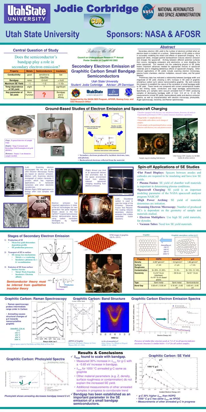
Jodie Corbridge . Utah State University Sponsors: NASA & AFOSR. Production. Production of SE Mean free path determines deposition profile SE production processes Transport of SE to surface SE energy loss mechanisms Metals: e - -e - scattering

E N D
Jodie Corbridge. Utah State UniversitySponsors: NASA & AFOSR Production • Production of SE • Mean free path determines deposition profile • SE production processes • Transport of SE to surface • SE energy loss mechanisms • Metals: e--e- scattering • Insulators: phonons & e--h+ recombination • Emission of SE from surface • Surface barrier • Metal: Work Function • Insulators: Electron affinity Transport Emission Studies in USU vacuum chamber Satellite moving through ambient plasma (Top): Exposed interior of sample stage. (Right): Stage Carousel and Retarding Field hemispherical grid (RFHG) (Bottom): Empty 1 cm diameter sample module • g-C 30% higher dmax than HOPG • 1050 °C g-C has same dmax as HPOG • Measurements of other annealed g-C in progress Abstract Presence of similar fine structure peak at 7±1 eV in all spectra indicates electronic structure is similar below ~5 eV for all carbon samples. Secondary electron (SE) yield is the number of electrons emitted when an electron beam is incident on a surface. Determination of SE yields is critical in accurately modeling the extent and effects of spacecraft charging. As a spacecraft orbits, charged particle bombardment induces electron emission and charges the spacecraft. Arching between different potential surfaces then occurs, damaging computers and electronics, or even disabling the entire spacecraft. Our research into the underlying physics of SE yields fosters important advances needed for appropriate choices of spacecraft materials and in mitigating deleterious effects of spacecraft charging. Other relevant applications of SE yields include scanning electron microscopy, plasma fusion chambers, electron multipliers, vacuum tubes, and flat panel displays. Preliminary data has indicated a relationship between bandgap width and magnitude of SE yield, showing a 30% increase in SE yield of graphitic amorphous carbon (g-C) above nanocrystalline graphite. My work extends this research to establish the nature of the correlation of small bandgap width to SE yield. These trends are compared with current semiempirical models of two limiting cases, conductors and large bandgap semiconductors. Specifically, g-C samples were vacuum annealed from 0º-1050º, producing samples of decreasing bandgap width of from ~0.5 eV to ~0 eV. My measurements include SE yields, backscattered yields and electron emission spectra, as well as characterization with electron microscopy, photoyields, Auger spectroscopy, resistivity, and Raman spectroscopy. Central Question of Study Electron interactions with materials Council on Undergraduate Research 7th Annual Poster Session on Capitol Hill 2003 Does the semiconductor’s bandgap play a role in secondary electron emission? Secondary Electron Emission of Graphitic Carbon Small Bandgap Semiconductors Utah State University Student: Jodie CorbridgeAdvisor: JR Dennison Supported by the NASA SEE Program, AFOSR, Boeing Corp. and USU Research Office Spin-off Applications of SE Studies • Flat Panel Displays: Spacers between anodes and cathodes are required to be insulating and have low SE yields. • Plasma Fusion: SE yield of chamber wall materials is important in determining plasma conditions. • Spacecraft Charging: SE yield is an important modeling parameter of the NASA spacecraft analyzer program NASCAP. • High Power Arching: SE yield of materials determines arc initiation. • Scanning Electron Microscopy: Number of produced SE’s is dependent on the geometry of sample and materials studied. • Electron Multipliers: Use high SE yield materials, for dynodes. • Vacuum Tubes: Need low SE yield materials. Chamber equipped with electron, ion, and photon beams, detectors, & analysis Experiments performed in UHV to ensure material cleanliness capabilities • Stage holds 11 samples/devices • Detachable cable allows swift change of samples • Each sample can be positioned before various detectors and electron, ion, and photon sources USU Fatman UHV chamber for SE/BSE studies & surface analysis Sample stage & retarding field detector (Left) Scanning electron microscopes like the one at the USU Electron Microscopy Facility are based on electron emission. (Bottom Left) Scanning electron micrograph of carbon nanotube Y junction which has important applications in nanoscale transistors and other electronic nanodevices. (Bottom Right) SEM applications in biology often coat samples with carbon. (Right) Almost one third of all spacecraft failures and anomalies due to the space environment result from plasma-induced spacecraft charging resulting from electron emission. (Left) Disordered carbon is used to coat the inside of the Princeton Tokamak Fusion Test Reactor. The coating reduces secondary electron emission that inhibits controlled fusion reactions. Electron emission has important applications in state-of-the-art technologies for next generation flat panel displays. Shown above is the first HyFEDTM (hybrid field emission device) demonstration device using carbon nanotubes developed by Applied NanoTech, Inc. • Secondary electrons produced by incident electrons, ions, and photons. • Backscattered electrons reflected from the material. Graphite Graphitic amorphous carbon (g-C) Stages of Secondary Electron Emission Annealing at: 350 °C 650 °C 850 °C 1050 °C 1050 °C g-C 0.1 eV HOPG 0.0 eV g-C 0.6 eV Photoyield shows annealing decreases bandgap toward 0 eV. Semiconductor theory must be inferred from qualitative insulator theory Graphitic Carbon Electron Emission Spectra Graphitic Carbon: SE Yield Graphitic Carbon: Raman Spectroscopy Graphitic Carbon: Band Structure • Raman spectroscopy probes intermediate range order in Carbon • Annealing causes structural changes of g-C towards nanocrystalline graphite Annealed ~1 hr at: 0 °C 350 °C 650 °C 850 °C 1050 °C ARPES of Graphite McGovern, Eberhardt, Plummer & Fisher, Physica 99B, 415 (1980). (e,2e) of annealed g-C Kurp, Canney, Vos, Kheifets & Weigold, JESRP, 87,231, (1998). Raman spectra taken by Tim Dallas and Mark Holtz at Texas Tech [3] Results & Conclusions • dmax found to scale with bandgap. • Measured 30% increase in dmax for g-C with a ~0.65 eV increase in bandgap. • dmax for 1050 °C annealed g-C same as graphite • Other material parameters (e.g. Z, density, surface roughness or contamination) do not explain the increased SE yield. • Additional measurements of other annealed samples in progress to corroborate trend • Bandgap has been established as an important parameter in the SE emission of a small bandgap semiconductors. Ground-Based Studies of Electron Emission and Spacecraft Charging STM image of graphite. (30 Ǻ x 30 Ǻ ) Graphitic Carbon: Photoyield Spectra