Download

1 / 149
1.49k likes | 1.5k Vues
Sinhgad Academy of Engg. Kondhwa(Bk), Pune-48. Basic Electronics Engg. ( 104012 ). Mr. S.S.Shah. Basic Electronics Engg. Teaching Scheme Lecture : 3 Hrs./Week Practical : 2 Hrs./Week. Examination Scheme Paper : 50 Marks Online Exam : 50 Marks Term Work : 25 Marks. Syllabus.

E N D
Sinhgad Academy of Engg. Kondhwa(Bk), Pune-48 Basic Electronics Engg. (104012) Mr. S.S.Shah
Basic Electronics Engg. Teaching Scheme Lecture : 3 Hrs./Week Practical : 2 Hrs./Week Examination Scheme Paper : 50 Marks Online Exam : 50 Marks Term Work : 25 Marks
Syllabus Unit I : DIODE CIRCUITS 6L Half wave rectifiers, Full wave rectifiers, Power supply filters and Capacitor filters, Diode limiting (Clippers) and Clamping circuits, Voltage multipliers, Zener diode & its applications, LEDs and Photodiodes Unit II : Bipolar Junction Transistor (BJT) Circuits 6L BJT Structure & its operation with normal biasing, Transistor characteristics and parameters, DC operating point, Transistor as an amplifier, Transistor as a switch, Enhancement-type MOSFET Unit Ill: Linear Integrated Circuits 6L Introduction to operational amplifiers, Op-amp input modes and parameters, Negative feedback, Op-amp with negative feedback, Comparators, Summing amplifiers, Integrators and Differentiators, IC 555 timer as an oscillator, Voltage regulation, IC voltage regulators (Three pin).
Unit IV: Digital Electronics 6L Introduction, Digital signals, Basic digital circuits-AND, OR, NOT, NANO, NOR, EX-OR, Boolean algebra, Examples of IC gates, Standard representation for logic functions, Half adder, Full adder, Multiplexers, De-multiplexer, Flip-flops, I-bit memory cell, D flip-flop, Shift registers, Counters, Block diagram of Microprocessor and Microcontroller and their applications. Unit V: Power devices and Transducers 7L Power Devices: Basics of 4-layer devices: Silicon Controlled Rectifier (SCR), Diac and Triac. Transducers: Introduction, Electrical transducer, Selecting a transducer, Resistive transducer, Thermistor, Inductive transducer, Linear Variable Differential Transducer (LVDT), Load cell, Phototransistor, Temperature transducers, Flow measurement (Mechanical transducers) Application of transducers: Digital Thermometer, Weighing machine/Block diagrams). Unit VI: Electronic Communication 7L Importance of Communication System, The elements of a Communication System, Bandwidth requirement, IEEE frequency spectrum, Transmission media: Wired (Twisted pair, Coaxial & Optical fiber Cables) and Wireless, Need for modulation, Analog modulation schemes- AM & FM, Mobile communication system: Cellular concept, Simple block diagram of GSM system.
REFERENCES • Art of Electronics – Paul Horowitz, Cambridge LPE • Electronics Devices and Circuits An Introduction- Allen Mottershed, PHI • Digital Principles and Applications – A P Malvino, Donald Leech, Tata McGraw Hill Fourth Edition
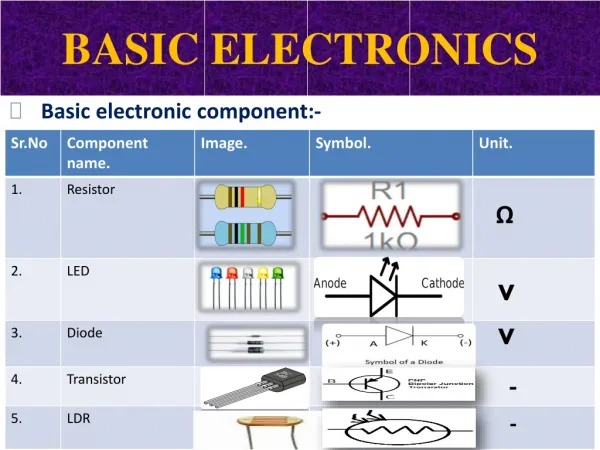
LIST OF PRACTICALS 1) Study of different electronic components. • Resistors ( Carbon Film, Metal Film, Wire Wound, Variable), b. Capacitors (Electrolytic, Mica, Ceramic, Variable), c. Inductors, Transformers, d. Connectors, Switches 2) Study of different electronic measuring instruments. a. To study different controls of DMM and measurement of parameters like AC and DC voltage, current b. To study controls of CRO, Measurements of frequency, phase, AC & DC Voltages. • To study various controls of a signal generator 3) Study of Regulated power supply. For a given Regulated Power Supply circuit with bridge Rectifier, capacitor filter and three terminal regulator: a. Identify pins of rectifier Diode (such as IN4001) and study of its data sheet specifications. b. Identify pins of Three Pin Regulator (such as LM 78XX or LM 79XX) and study of its data sheet specifications. c. To measure voltages and observe waveforms at transformer secondary, output of Bridge Rectifier, output 'of Regulator.
4) Study of Single stage BJT Common Emitter amplifier circuit. For a given BJT CE Amplifier circuit a. Identify pins ofa BJT (such as BC547) and study of its data sheet specifications. b. To measure voltages and observe waveforms at input and output terminals of single stage BJT Common Emitter amplifier circuit. • Calculate voltage gain of the amplifier. 5) Study of Op-amp based amplifiers circuits. a. Identify pins of an Opamp (such as LM74 I) b. Implement given voltage equation for 2 inputs with Oparnp based Summing and Difference amplifier (such as Vo=2V1+3V2 and Vo=4V1-V2) 6) Study of IC 555 Timer circuit. a. Identify pins of IC 555 Timer b. Observe output waveform and measure frequency of output wave for IC 555 Timer used in Astable mode. 7) Study of Digital circuits. a. Identify pins of Digital Logic Gates ICs such as AND, OR, NOT, Ex-OR, NAND • Implement Half and Full Adder circuit with basic logic gate Ics 8) Build and test Simple application circuit Build & Test any circuit using IC such as Oparnp LM74 I, IC 555 Timer, LM78XX/79XX or any digital logic gate IC.
COURSE OBJECTIVE By the end of the course, students will be able to: • To become acquainted with diode characteristics, different types of displays. • To become familiar with the bipolar junction transistor, FET, MOSFET. • TO become acquainted with digital electronics. • To become familiar with different types of transducers. • To become familiar with different communication systems. • To become acquainted with mobile communication systems. • To understand the basic concepts of Operational Amplifier & its applications. • To have hands on different measuring instruments for frequency, phase and amplitude measurement & soldering techniques.
INDEX Unit 1:Diode Circuits 1. Half wave rectifiers, Full wave rectifiers 2. Power supply filters and Capacitor filters 3. Diode limiting (Clippers) and Clamping circuits 4. Voltage multipliers 5. Zener diode & its applications 6. LEDs and Photodiodes
Applying voltage across pn Junction • The potential difference across a pn junction can be applied in two ways namely, • Forward biasing. 2. Reverse biasing.
Forward biasing • When external voltage applied to the junction is in such a direction that it cancels the potential barrier, thus permitting current flow, it is called “ forward biasing”. • To apply forward bias, connect positive terminal of the battery to p-type and negative terminal to n-type as shown in diagram.
Forward bias Depletion region - + - + electron holes - + - + Original barrier Electron flow - +
p n - + No external field External field
The applied forward potential establishes an electric field which acts against the field due to potential barrier. • Therefore, the resultant field is weakened and the barrier height is reduced at the junction as shown in figure (b). • As potential barrier voltage is very small (0.1 to 0.3V) a small forward voltage is sufficient to completely eliminate the barrier.
Once the potential barrier is eliminated by the forward voltage, junction resistance becomes almost zero and a low resistance path is established for the entire circuit. • Therefore, current flows in the circuit. This is called as “ forward current”.
With forward bias to pn junction, the following points are important: • The potential barrier is reduced and at the some forward voltage (0.1 to 0.3V) , it is eliminated altogether. 2. The junction offers low resistance (called forward resistance Rf ) to current flow. 3. Current flows in the circuit due to the establishment of low resistance path. The magnitude of current depends upon the applied forward voltage.
Reverse biasing • When the external voltage applied to the junction is in such a direction that potential barrier is increased, it is called “ reverse biasing”. • To apply reverse bias, connect negative terminal of the battery to p-type and positive terminal to n-type as shown in figure.
Reverse bias Depletion region P N - - + + - - + + - - + + - - + + Original barrier - + No electron flow
From the diagram it is clear that applied reverse voltage establishes an electric field which acts in same direction as the field due to potential barrier. • Therefore, the resultant field at the junction is strengthened and the barrier height is increased as shown in diagram. • The increased potential barrier prevents the flow of charge carriers across the junction. Thus a high resistance path is established for the entire circuit and hence the current does not flow.
With reverse bias to pn junction, the following points are important: • The potential barrier is increased. • The junction offers very high resistance (called reverse resistance Rr) to current flow. • No current flows in the circuit due to the establishment of high resistance path.
Conclusion • From the above discussion, it follows that with reverse bias to the junction, a high resistance path is established and hence no current flow occurs. • On the other hand , with forward bias to the junction, a low resistance path is setup and hence current flows in the circuit.
Current flow in a forward biased pn junction • Lets study how current flows across pn junction when it is forward biased. • Following figure shows a forward biased junction:
Forward bias junction p n - - + + - - + + - - + + - +
Under the influence of forward voltage, the free electrons in n-type move towards the junction, leaving behind positively charged atoms. • However, more electrons arrive from the negative battery terminal and enter the n-region to take up their places. As the free electrons reach the junction, they become valence electrons. • As valence electrons, they move through the holes in the p- region. The valence electrons move towards left in the p- region which is equivalent to the holes moving to right.
When the valence electrons reach the left end of the crystal, they flow into the positive terminal of the battery. • The mechanism of current flow in a forward biased pn junction can be explained as below: • The free electrons from the negative terminal continue to pour into the n- region while the free electrons in the n- region move towards the junction. 2. The electrons travel through the n- region as free electrons. i.e. current in n- region is by free electrons.
When these electrons reach the junction, they combine with holes and become valence electrons. • The electrons travel through p- region as valence electrons. i.e. current in the p- region is by holes. • When these valence electrons reach the left end of crystal, they flow into the positive terminal of the battery.
Conclusion • From the above discussion, it is concluded that in n- type region, current is carried by free electrons whereas in p-type region, it is carried by holes. • However, in the external connecting wires, the current is carried by free electrons.
Diode symbols • The symbols used for the different diodes and the direction of current flow associated with them, we will refer following figures. • It should be noted that the arrow in the semiconductor symbol points in the same direction as the conventional current flow in the forward biased condition.
Symbols for diodes P K P K Semiconductor diode Thermionic diode (+ indicates “cathode”) P K + Selenium diode
Semiconductor diode • A pn junction is known as a semiconductor or crystal diode. • The outstanding property of a semiconductor diode to conduct current in one direction only permits it to be used as rectifier. • A semiconductor diode is usually represented by the schematic symbol,
The arrow in the symbol indicates the direction of easier conventional current flow. • Semiconductor diode has two terminals when it is connected in a circuit, one thing to decide is whether the diode is forward or reverse biased. • If the external circuit is trying to push the conventional current in the direction of arrow, the diode is forward biased. • On other hand, if the conventional current is trying to flow opposite to arrowhead the diode is reverse biased.
Semiconductor diode as a Rectifier Vin Vout 50 V 50 V Vin RL 0 Vout t t
The a.c input voltage to be rectified, the diode and load RL are connected in series. • The d.c output is obtained across the load as explained in following discussion. • During the positive half cycle of a.c input voltage, the arrowhead becomes positive w.r.t bar. • Therefore, diode is forward biased and conducts current in the circuit.
The result is that positive half cycle of input voltage appears across RL as shown. • However, during negative half cycle of input a.c voltage, the diode becomes reverse biased because now the arrowhead is negative w.r.t bar. • Therefore, diode does not conduct and no voltage appears across load RL . • The result is that output consists of positive half cycles of input a.c voltage while the negative half cycles are suppressed.
In this way, semiconductor diode has been able to do rectification. i.e. change a.c into d.c. here output across RL is pulsating d.c. • The behavior of diode is like a switch. When the diode is forward biased, it behaves like a closed switch and connects the a.c supply to the load RL. • However, when the diode is reversed biased it behaves like an open switch and disconnects the a.c supply from the load RL. • This switching action of diode permits only the positive half cycles of input a.c voltage to appear across RL.
Semiconductor diode rectifiers • When a d.c supply is required, the mains a.c supply is rectified by using semiconductor diodes. The following two rectifier circuits can be used. • Half - wave rectifier. 2. Full -wave rectifier.
Half wave rectifier • In half-wave rectification, the rectifier conducts current only during the positive half cycles of input a.c supply. • The negative half-cycles of supply are suppressed. i.e. during negative half cycles, no current is conducted and hence no voltage appears across the load. • Therefore, current always flows in one direction (i.e. dc) through the load though after every half- cycle.
Circuit description • The figure shows the circuit where a single semiconductor diode acts as a half–wave rectifier. • The a.c supply to be rectified is applied in series with the diode and load resistance RL .Generally, a.c supply is given through a transformer. The use of transformer permits two advantages. • Firstly, it allows us to step up or step down the a.c input voltage as the situation demands. • Secondly, the transformer isolates the rectifier circuit from power line and thus reduces the risk of electric shock.
Operation • The a.c voltage across the secondary winding AB changes polarities after every half-cycle. During positive half cycle of input a.c voltage , end A becomes positive w.r.t end B. • This makes diode forward biased and hence it conducts current. During the negative half cycle, end A is negative w.r.t end B. Under this condition the diode is reverse biased and it conducts no current. • Therefore, current flows through the diode during positive half cycles of input a.c voltage only, it is blocked during the negative half-cycles.
Half-wave Rectifier Circuit D i A A.C. supply Vin RL Vout B
Vin 0 t Vout 0 t i 0 t
In this way, current flows through the load RL always in the same direction. Hence d.c output is obtained across RL. • It may be noted that output across the load is pulsating d.c. these pulsations in the output are further smoothened with the help of filter circuits.
Efficiency of Half-wave rectifier • The ratio of d.c power output to the applied input a.c power is known as rectifier efficiency. • i.e. Rectifier efficiency, η =
d.c power • The output current is pulsating direct current. Therefore, in order to find d.c power, average current has to be found out. • Iav = Idc = = • = • =
Now, = • = • Therefore, d.c power, Pdc = × RL • = × RL
a.c power input • The a.c power input is given by, • Pac = , • For a half –wave rectified wave, Irms = Pac =
Rectifier efficiency = = = =
The efficiency will be maximum if rf is negligible as compared to RL .Therefore maximum rectifier efficiency = 40.6 %. This shows that in half-wave rectification a maximum of 40.6 % of a.c power is converted into d.c power.
DC output voltage • The dc output voltage appearing across RL will be, • Vdc = Idc RL , which can be put in terms of Vm by substituting the expression for Idc and Im. • V dc = Idc RL ….. (i) • Which can be put in terms of Vm by substituting the expression for Idc & Im Vdc = Idc RL = RL
= • = • Thus if RL ˃˃ RS + Rf the output voltage is, • Vdc = , Alternatively, Idc = =