Download
1 / 17
170 likes | 364 Vues
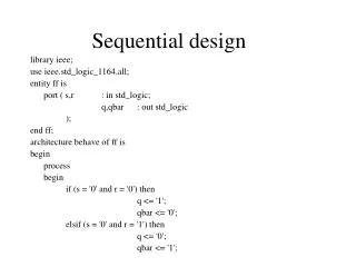
Sequential Design. ELEC 311 Digital Logic and Circuits Dr. Ron Hayne Images Courtesy of Cengage Learning. Sequential Circuits. Design Example. 2-bit Variable Counter. State Assignment: Q1 Q0 = Z1 Z0. Transition Table (1). Transition Table (1). Transition Table (1).

E N D
Sequential Design ELEC 311 Digital Logic and Circuits Dr. Ron Hayne Images Courtesy of Cengage Learning
Sequential Circuits 311_16
Design Example • 2-bit Variable Counter State Assignment: Q1 Q0 = Z1 Z0 311_16
Transition Table (1) 311_16
Transition Table (1) 311_16
Transition Table (1) 311_16
Transition Table (2) 311_16
Transition Table (2) 311_16
Transition Table (2) 311_16
Next State (FF) Equations • D1(X1,X0,Q1,Q0) = Q1+ = Σm(0,3,5,6,8,11,13,14) • D0(X1,X0,Q1,Q0) = Q0+ = Σm(0,2,4,6,12,13,14,15) • D1 = (X0′·Q1′·Q0′) + (X0·Q1′·Q0) + (X0′·Q1·Q0) + (X0·Q1·Q0′) • D0 = (X1′·Q0′) + (X1·X0) 311_16
Xilinx CPLD Implementation 311_16
Xilinx FPGA Implementation 311_16
UNISIM Library Components • FDC • D Flip-Flop with Asynchronous Clear component FDC port (Q : out STD_LOGIC; C : in STD_LOGIC; CLR : in STD_LOGIC; D : in STD_LOGIC); end component; 311_16
VHDL Package • project4_pkg.vhd • Clock Divider component CLK_DIV port(CLK_IN : in std_logic; CLK_OUT : out std_logic ); end component; 311_16
VHDL Model library UNISIM; use UNISIM.VComponents.all; use work.Project4_Pkg.all; entity Counter is Port ( X : in std_logic_vector(1 downto 0); CLR : in std_logic; CLK : in std_logic; Z : out std_logic_vector(1 downto 0)); end Counter; architecture DATAFLOW of Counter is signal D : std_logic_vector(1 downto 0); signal Q : std_logic_vector(1 downto 0); signal SLOW_CLK : std_logic; 311_16
VHDL Model begin D(1) <= (not X(0) and not Q(1) and not Q(0)) or (X(0) and not Q(1) and Q(0)) or (not X(0) and Q(1) and Q(0)) or (X(0) and Q(1) and not Q(0)); D(0) <= (not X(1) and not Q(0)) or (X(1) and X(0)); CDIV : CLK_DIV port map (CLK, SLOW_CLK); FF1 : FDC port map(Q(1), SLOW_CLK, CLR, D(1)); FF0 : FDC port map(Q(0), SLOW_CLK, CLR, D(0)); Z <= Q; end DATAFLOW; 311_16
Summary • Design Example • Functional Description • Transition Table • Next State Equations • FPGA Implementation • VHDL Model 311_16