Download
1 / 19
230 likes | 581 Vues
Studies of Gamma Radiation Induced Effects in Ge -rich Chalcogenide Thin Films .

E N D
Studies of Gamma Radiation Induced Effects in Ge-rich Chalcogenide Thin Films D. Nesheva1, M. Ailavajhala2, P. Chen2, D. A. Tenne3, H. Barnaby4, M. Mitkova2*1Institute of Solid State Physics, Bulgarian Academy of Science, 1784 Sofia, Bulgaria1Dept. of Electrical and Computer Engineering, Boise State University, Boise, ID 83725, USA3 Dept. of Physics, Boise State University, Boise, ID 83725-1570, USA4 School of Electrical, Computer, and Energy Engineering, Arizona State University, Tempe, AZ 85287-5706, USA
Outlines • Motivation • Experimental details • Raman scattering data • Dark and photoconductivity data • Conclusions
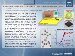
Chalcogenide glasses These glasses are based on the chalcogen elements S, Se, and Te and are formed by the addition of other elements such as Ge, As, Sb, Ga, etc. They are: • generally transparent from the visible up to infrared; • show phase change memory effects; • can be doped by rare-earth elements and numerous applications of active optical devices have been proposed; • are optically highly non-linear and could therefore be useful for all-optical switching; • are sensitive to the absorption of electromagnetic radiation and particle irradiation and show a variety of photoinduced effects as a result of illumination: photodarkening, photobleaching, photocrystallization, photoplastic effects, etc.
Photodiffusionin Chalcogenide Glasses EC Ag+ EF EV Ag film Ag film Glass film Scheme of electron/ion generation at the metal/metal-doped chalcogenide interface Radiation sensor, BSU February 24, 2011
Experimental details • Synthesis of bulk Ge40Se60 glasses and thermal evaporation in vacuum, film thickness 100 nm. • EDS composition check by a LEO 1430VP Scanning Electron Microscope with EDS accessory. • Gamma irradiation in a closed cylindrical cavity by concentrically established60Co (average energy E = 1.25 MeV) radioisotope capsule at a dose rate of 12 rad/sec. The applied γ-ray doses were ranging from 20 krad(Si) to 3 Mrad(Si). • Raman scattering measured by a Horiba JobinYvon T64000 triple monochromator, = 441.6 nm blue line of a He-Cdlase, power 60 mW on ~ 0.2 mm diameter circle area, Tm=100K. • Electrical conductivitymeasured in the 293-423 K range; co-planar aquadag (carbon) contacts on the top surface of the layers; the contacts produce a gap cell with an active area of ~ (110) mm2.
There are two types of effects occurring in chalcogenide glasses upon –irradiation*: • reversible which decay after ceasing the radiation • irreversible which are stable with the time. The reported measurements have been carried out after the radiation has been stopped, so that they can be regarded as capturing only the irreversible changes caused by radiation. * O. I. Shpotyuk, in Semiconducting Chalcogenide Glass I: Glass formation, Structure and simulated transformations in chalcogenide glasses, edited by R. Fairman and B. Ushkov (Elsevier Academic Press, New York, 2004), p. 215.
Raman scattering Raman scattering spectra (symbols) of virgin and -irradiated Ge40Se60 films: (a) low-dose range, (b) high-dose range. The dashed lines represent the deconvolution results for the samples irradiated with 100 krad (a) and 1.3 Mrad (b).
GeSe2 – main Raman modes Symmetric, 150-230 cm-1 ETH units Se3-Ge-Ge-Se3 178 cm-1 216 cm-2 Asymmetric 230-330 cm-1
Raman scattering – symmetric vibrations Dependence of the area ratio ES/CS structural units for Ge40Se60 films at different irradiation doses. Results from different evaporation batches are presented. Irradiation induced decrease of the ethane-like units i.e. of the weakest Ge-Ge bonds.
Raman scattering Raman scattering spectra (symbols) of virgin and -irradiated Ge40Se60 films: (a) low-dose range, (b) high-dose range. The dashed lines represent the deconvolution results for the samples irradiated with 100 krad (a) and 1.3 Mrad (b).
Raman scattering – asymmetric vibrations Relative variation of the integrated intensity of the scattered light in the 230-330 cm-1 range with respect to the sum of the integrated intensities of the corner-shared (ICS) and edge-shared (ICS) modes. Each group of symbols corresponds to different evaporation batch.
Dark and photoconductivity Temperature dependences of dc dark conductivity and steady-state photoconductivity of virgin and -irradiated (dose of 3 Mrad) Ge40Se60 thin films. The solid lines represent a linear fit of the experimental points (symbols).
Conclusions • In Ge40Se60 thin films the gamma irradiation induces : • decrease of the weakest Ge-Gebonds; • increase in the ES/CS ratio and at high irradiation doses an overall disorder decrease. Both effects could be important for Ag diffusion in the films; • The disorder decrease is similar to the effect of the temperature treatment but it is related to strong electron-phonon interaction rather than to sample heating.
Interaction of “pure”Chalcogenide glasses with electromagnetic radiation Radiation sensor, BSU February 24, 2011
Gamma-induced optical changes in GeSe thin films Absorption spectra of (1,2) gamma-irradiated and (3) unirradiated a-GeSe films (1.25 m)(a) before and (b) after storage for a year; D= (1)1 MGy and (2) 10 kGy. (1, 2) Eopt and (3, 4) n as functions of gamma dose for a-GeSe films (2, 3) before and (1, 4) after storage for a year. R. R. Romanyuk et al., Inorganic Materials, 2007, Vol. 43, No. 6, pp. 584–587.
Chalcogenide glasses These glasses are based on the chalcogen elements S, Se, and Te and are formed by the addition of other elements such as Ge, As, Sb, Ga, etc. They • are generally transparent from the visible up to infrared • can be doped by rare-earth elements and numerous applications of active optical devices have been proposed. • are optically highly non-linear and could therefore be useful for all-optical switching. • are sensitive to the absorption of electromagnetic radiation and particle irradiation and show a variety of photoinduced effects as a result of illumination: photodarkening, photobleaching, photocrystallization, photoplastic effects, etc. 3D AFM picture (a) and a cross-section (b) of the pattern obtained on 0.5 lm thick a-Se layer irradiated with 60 keV Xe24+ ions. 3D AFM picture (a) and a cross-section (b) of the pattern recorded on Se/As2S3 nanolayered film with total thickness d = 900 nm, illuminated through a microgrid with a 17 mW, 532 nm diode laser for 30 min. S. Kokenyesi et al. / Journal of Non-Crystalline Solids 353 (2007) 1470–1473.
Cross Section of a Pixel of a X-ray Imaging Array S. A. Kasap, J.A. Rolands, IEE Proc. Circuits Devices Syst., 149 (2002) 85. Radiation sensor, BSU February 24, 2011
Solid electrolyte The solid state electrolyte material is formed by Ag diffusion in Ge - Chalcogenide glasses (ChG). This electrolyte allows the movement of silver ions under the influence of an electric field. The electrically stimulated injection and removal of metal in the solid electrolyte at very low voltage is the basis of Programmable Metallization Cell memory PMCmdevices technology. Schematic of (a) PMCm device modeled as an electrochemical cell. a. Unwritten device. (b) Device during WRITE: A very small voltage rapidly “injects” into the electrolyte excess silver ions, which are reduced by the electron current to form highly stable silver dendrites within the electrolyte. (c) Written Device: The electrondeposition process stops when a conducting link is formed. Metallic link reduced the resistance of the structure by many orders of magnitude.(d) Device during ERASE: A very small reverse voltage (a few hundred mV) removes excess silver from the electrolyte. Excess silver is backed on the silver electrode by an easily reversible reaction.