Download
1 / 56
850 likes | 1.71k Vues
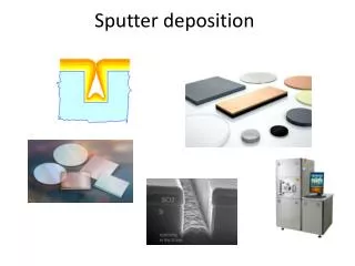
Sputter deposition of Thin Films. Course Tutor Dr R E Hurley. Northern Ireland Semiconductor Research Centre School of Electrical & Electronic Engineering The Queen’s University of Belfast. Course content. Applications Definitions Advantages of sputtering Physical principles

E N D
Sputter deposition of Thin Films Course Tutor Dr R E Hurley Northern Ireland Semiconductor Research Centre School of Electrical & Electronic Engineering The Queen’s University of Belfast
Course content • Applications • Definitions • Advantages of sputtering • Physical principles • The glow discharge • Types of sputtering system • Magnetron sputtering • Process parameters (effects on thin film properties) • Stress in films • Microstructure • Uniformity considerations • Etching • Compounds and reactive sputtering • Examples of systems
Application examples of sputtering • Developed in last 30yrs into a sophisticated coating tool • Optical-interference filters and protective coatings for • lenses, mirrors, transparent conductive coatings (ITO), • for displays, heat filters for architectural glass • Mechanical -hard coatings for tools, low friction coatings • for bearing surfaces, anti-corrosion coatings in aircraft industry • Electronics - especially semiconducting industry, metallisation, • barrier layers, display circuitry, discrete components • Data storage - CDs, DVDs, RW heads
Sputtering for thin films • Q. What is sputtering? • A. The removal of material (normally as atoms), from the • surface of a target by energetic ion (or neutral) bombardment. • The source of ions may be an electrical plasma discharge • surrounding the target, or alternatively a separate ion-source. • The incident ions cause cascades of collisions within the target, • where these intersect the surface, sputtering occurs. • A receiver, (substrate), collects the sputtered atom flux as a thin film.
Advantages of sputtering • Versatility • Wide range of materials including compounds, • alloys, and high purity targets available and interchangeable • Control • Particularly in the case of compounds and alloys when problems • of fractionation do not occur. • Good stability and control over deposition rate • Mass flow and pressure controllers work well.(Even without these, • good repeatability is possible once a system has achieved equilibrium) • Scalability • Substrates can be very small or very large, discrete or continuous as a roll
Types of sputtering systems • Diode (1960s, slow, rather high pressure [~0.1mb], • secondary electrons at substrate, tendency to arc, conducting targets only) • R.F. (60s,70s, good for insulators, slow, • lower pressure than diode, [~0.005 mb], secondary electrons at substrate) • Magnetron (DC and RF) (late 70s, 80s) • (the modern system, fast [minimising contamination], low pressure • [minimal pump throttling needed hence improved pumping of contaminants], • no secondaries to heat substrate) • Ion beam (for ultra-clean work, research, slow,) • Hybrids (all types of combination system, • may include evaporation, microwave sources etc.)
Problems with DC sputtering • Relatively high pressure overloads pumps, means • contamination, lack of control over process. • Bombardment of substrate by energetic neutrals and -ve ions (contamination) • Bombardment of substrate by energetic secondary electrons (heating) • Cannot be used with insulating targets; arcing by surface charging • Low deposition rate (increases contamination)
Alternatives to DC Sputtering • Reduce working pressure (increase plasma density • for a given working pressure), by additional excitation: • R.F. (13.56MHz) • 2. External magnetic coils. • 3. Use an ion beam system in UHV (very slow) • 4. Magnetron sputtering - has become the industry norm.
Magnetron sputtering • High deposition rates • (good for production, minimises effect of contaminants • Low pressure operation • (minimal throttling of pump, means higher pump speed • and less contaminants. • Elimination of secondary electrons on substrates • (Plastics and heat-sensitive substrates can be coated, • the substrate temperature can be regulated as required. • Good control over reactive sputtering • (high pumping speed = stability and control)
Magnetron sputtering Unbalanced Balanced
Sputtering parameters • Deposition rate (Å/sec, micron/min) • Substrate temperature • Gas pressure/plasma type (DC, RF, microwave, hot filament) • Target/substrate geometry, relative motion (uniformity)
Sputtering – thin film properties affected • Stress • Crystallinity/amorphousness • Gas and other impurity incorporation • Density and structure • Stoichiometry or composition • Effect of all above on optical, electrical, magnetic or mechanical properties.
Illustration of stress in films Film ‘wants’ to be ‘larger’ Film ‘wants’ to be ‘smaller’
Causes of stress in thin films • 1. Thermal Stress • differences in expansion coefficient between film and substrate • 2. Intrinsic Stress • incorporation of gas atoms • mismatch during epitaxy • recrystallisation • phase transformations • microscopic voids, porosity, and dislocation effects. • atomic peening • Tensile stress associated with voids and porosity • Compressive stress associated with gas atom incorporation • and atomic peening.
Stress in thin films Mechanism for compressive stress in sputtering (Thornton and Hoffman, 1985)
Stress in thin films - pressure effect K. O'Donnell, J. Kostetsky, and R.S. Post of NEXX Systems LLC TiW (heavy mass, atomic peening effect at low pressures) Hoffman and Thornton, 1979)
Effect on input power on stress, DC,AlN,sputtered Kusaka, vac2000,59,812
Effect of negative bias on stress,, Cr, NiV (RF sputtered) K. O'Donnell, J. Kostetsky, and R.S. Post of NEXX Systems LLC, 2002 Use of bias to reduce stress to near zero (more dense microstructure)
Microstructure of thin films • Affected by energy input into substrate during deposition • Increasing energy promotes grain growth and crystallisation • Gas pressure affects energetic neutral component. • Substrate temperature • Substrate bias affects energy of bombarding ions
Magnetron sputtering - microstructure diagram Microstructure as a function of argon pressure and substrate temperature Movchan and Demchishin, 1969
Use of AFM for roughness measurement Sputtered AlN. AFM showing roughness v. power Kusaka et al. Vac 2000,59, 810
Film uniformity in sputtering • Non-uniformity is a potential problem in magnetron sputtering • (caused by shape of the magnetic field lines which depend on design used) • In semiconductor processing of 300 mm wafers for ULSI the problem is acute.
Solutions for non-uniformity • Use relative motion of target and substrate • For rotation over circular targets, +/- 8% is typical for many systems • For circular targets, sun and planets will reduce to < 1% • For large systems, lateral (shuttle), motion over rectangular targets is good • These systems are used for architectural glass and roll-coating of plastic sheet but also for batches of smaller components, e.g. silicon wafers
RF Mag. with sun and planets holders for ZnO films for SAW filters, Ar/O2. (Yoshino et al Vac.2000,59, 538-545)
In-line reactive sputtering for ITO, dc and mf Strumpfel and May, Vacuum, 59, 2000, 500-505
Industrial magnetrons for coating Cu, MF-pulsed for solar absorb. 1m wide at 1m/min.Cr-carbide, Milde etal. Vac.,2000,59, 825-35
Use of sputtering for etching substrates • Place substrate on target → controlled etching • Dedicated etchers are normally used with or without chemistry • Vertical side-walls are possible (anisotropic etching) • Reactive chemistry (Br, Cl, O2), increases etch-rate • but increases isotropy • A mask allows pattern delineation, but leads to tapering and trenching • A separate broad-area ion source may be used
Use of sputtering for etching substrates Sputter etch Wet chemical etch
Sputtering of compounds • Compounds of two or more components are possible • Methods • Several targets (co-sputtering) • Compound or alloy target • (Note:components sputter at different rates, but an equilibrium will be established • after a certain time which results in composition of original target material being • deposited as a thin film. The exception is when component is released as a gas • (O2, N2), and hence depleted from depositing film.) • Multi-component target (discrete pieces of second material)
ZrTi target/PbO pellets, rf diode PZT ferroelectrics Kim et a. Vacuum, 59,2000 559-566
Reactive sputtering for oxides and nitrides • The main problem is control: • The critical reaction occurs at the target surface • A mixture of argon and reactive gas (O2, N2) is used. • Too much reactive gas, sputter-yield falls, gas build-up uncontrollably and deposited layer is gas-rich. • Too little reactive gas, sputter-yield increases uncontrollably and layer is metal-rich
Control problem in reactive sputtering Hysteresis effect during reactive sputtering, (Sproul, 1984) • The partial pressure follows a hysteresis loop with gas flow supply. • The operating point for stoichiometric films is at a point of abrupt change of slope.
Reactive sputtering of oxides and nitrides • Methods of controlling the process: • Setting the flow/pressure at fixed values and using trial and error • Unsatisfactory, may work with a high-speed pumping system. • Plasma monitoring using OpticalEmission Spectrometry • Works well and costs can be moderate with CCD system. • With fast enough pumping, manual ‘tweaking’ is OK. • A more sophisticated system will use feedback from spectral • lines to control flow ratio of argon/reactive gas, and a • pressure controller to control total pressure.
Optical emission spectrometry (OES) • Suitable spectral lines of M and O2 (or N2) • These are normally in the near UV and a quartz window is necessary. • The ratio of the two lines is held at a fixed value by adjustment of the Ar/reactive gas flows. • The ratio can be chosen for stoichiometry or metal or gas rich films as required.
Optical emission spectroscopy Library file, Ti(I)
Optical emission spectroscopy Reactive sputtering of ZrN showing effect of varying N2 flow-rate (Berg et al., 1986) Ar N2 Zr
Biased directional sputtering (Sato et al, Vacuum 59, 2000,437-444) Ti, Ta comps. Barrier layers
RF magnetron system for ferroelectric films (Ichikawa et al. Vacuum,59, 2000, 417-423) PbT and SrT effect of 02 partial pressure in Ar on film growth.