Download
1 / 1
20 likes | 188 Vues
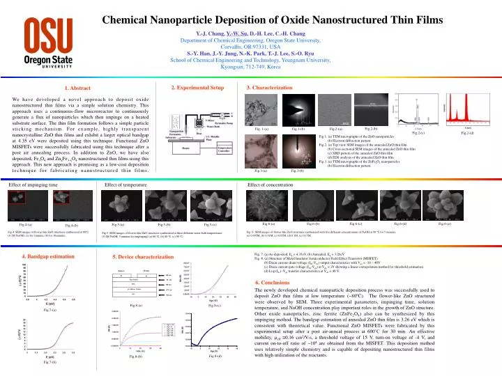
Drain. Source. 300 nm. Al. Al. 24 nm. Zinc Oxide. SiO 2. 100 nm . p+ Silicon (Gate). 675 m m . Au. 500 nm. Chemical Nanoparticle Deposition of Oxide Nanostructured Thin Films. Y.-J. Chang , Y.-W. Su , D.-H. Lee, C.-H. Chang

E N D
Drain Source 300 nm Al Al 24 nm Zinc Oxide SiO2 100 nm p+ Silicon (Gate) 675 mm Au 500 nm Chemical Nanoparticle Deposition of Oxide Nanostructured Thin Films Y.-J. Chang,Y.-W. Su, D.-H. Lee, C.-H. Chang Department of Chemical Engineering, Oregon State University, Corvallis, OR 97331, USA S.-Y. Han, J.-Y. Jung, N.-K. Park, T.-J. Lee, S.-O. Ryu School of Chemical Engineering and Technology, Yeungnam University, Kyongsan, 712-749, Korea 2. Experimental Setup 3. Characterization 1. Abstract 200 nm We have developed a novel approach to deposit oxide nanostructured thin films via a simple solution chemistry. This approach uses a continuous-flow microreactor to continuously generate a flux of nanoparticles which then impinge on a heated substrate surface. The thin film formation follows a simple particle sticking mechanism. For example, highly transparent nanocrystalline ZnO thin films and exhibit a larger optical bandgap at 4.35 eV were deposited using this technique. Functional ZnO MISFETs were successfully fabricated using this technique after a post air annealing process. In addition to ZnO, we have also deposited, Fe3O4 and ZnxFe3-xO4 nanostructured thin films using this approach. This new approach is promising as a low-cost deposition technique for fabricating nanostructured thin films. Fig.2-(b) Fig. 1-(a) Fig.1-(b) Fig.2-(a) Fig.2-(c) Fig.2-(d) Fig.1. (a) TEM micrographs of the ZnO nanoparticles (b) Electron diffraction pattern Fig.2. (a) Top view SEM images of the annealed ZnO thin film (b) Cross-sectional SEM images of the annealed ZnO thin film (c) XRD pattern of the annealed ZnO thin film (d) EDS analysis of the annealed ZnO thin film Fig.3. (a) TEM micrographs of the ZnFe2O4 nanoparticles (b) Electron diffraction pattern Fig.3-(a) Fig.3-(b) 200 nm Effect of impinging time Effect of temperature Effect of concentration Fig.6-(a) Fig.6-(b) Fig.6-(c) Fig.6-(d) Fig.6-(e) Fig.4-(a) Fig.5-(a) Fig.5-(b) Fig.5-(c) Fig.4-(b) Fig.4. SEM images of flower-like ZnO structures synthesized at 90℃ (0.1M NaOH); (a) for 1minute, (b) for 10minutes. Fig. 6. SEM images of flower-like ZnO structures synthesized with five different concentrations of NaOH at 90 ℃ for 5 minutes (a) 0.005M, (b) 0.01M, (c) 0.05M, (d) 0.1M, (e) 0.15M Fig.5. SEM images of flower-like ZnO structures synthesized at three different water bath temperatures (0.1M NaOH, 5 minutes for impinging) (a) 60 ℃, (b) 80 ℃, (c) 90 ℃. Fig. 7. (a) As-deposited, Eg = 4.35eV, (b) Annealed, Eg = 3.26eV Fig. 8. (a) Structure of Metal Insulator Semiconductor Field Effect Transistor (MISFET) (b) Drain current-drain voltage (Ids-Vds) output characteristics with Vgs = -10 ~ 40V (c) Drain current-gate voltage (Ids-Vgs) at Vds = 1V showing a linear extrapolation method for threshold estimation (d) Log (Ids)–Vgs transfer characteristics at Vds = 40 V. 4. Bandgap estimation 5. Device characterization 6. Conclusions The newly developed chemical nanoparticle deposition process was successfully used to deposit ZnO thin films at low temperature (~80ºC). The flower-like ZnO structured were observed by SEM. Three experimental parameters, impinging time, solution temperature, and NaOH concentration play important roles in the growth of ZnO structure. Other oxide nanoprticles, zinc ferrite (ZnFe2O4) also can be synthesized by this impinging method. The bandgap estimation of annealed ZnO thin film is 3.26 eV which is consistent with theoretical value. Functional ZnO MISFETs were fabricated by this experimental setup after a post air-anneal process at 600˚C for 30 min. An effective mobility, eff0.16 cm2/V-s, a threshold voltage of 15 V, turn-on voltage of -4 V, and current on-to-off ratio of ~104 are obtained from the MISFET. This deposition method uses relatively simple chemistry and is capable of depositing nanostructured thin films with high utilization of the reactants. Fig.8-(a) Fig.8-(c) Fig.7-(a) Fig.8-(d) Fig.8-(b) (201) Fig.7-(b)