Download
1 / 23
230 likes | 454 Vues
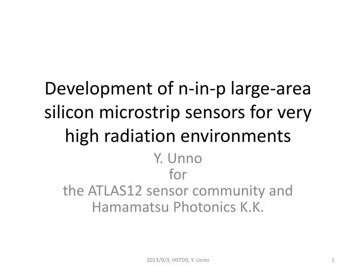
Development of n-in-p large-area silicon microstrip sensors for very high radiation environments. Y. Unno for the ATLAS12 sensor community and Hamamatsu Photonics K.K. ATLAS Tracker Layouts. Current inner tracker Pixels: 5-12 cm Si area: 2.7 m 2 IBL(2015): 3.3 c m

E N D
Development of n-in-p large-area silicon microstrip sensors for very high radiation environments Y. Unno for the ATLAS12 sensor community and Hamamatsu Photonics K.K. 2013/9/3, HSTD9, Y. Unno
ATLAS Tracker Layouts • Current inner tracker • Pixels: 5-12 cm • Si area: 2.7 m2 • IBL(2015): 3.3 cm • Strips: 30-51 (B)/28-56 (EC) cm • Si area: 62 m2 • Transition Radiation Tracker (TRT): 56-107 cm • Occupancy is acceptable for <3x1034 cm-2s-1 • Phase-II at HL-LHC: 5x1034 cm-2s-1 • Phase-II upgrade (LOI) • Pixels: 4-25 cm • Si area: 8.2 m2 • Strips: 40.-100 (B) cm • Si area: 122 (B)+71(EC)=193 m2 • Major changes from LHC • All silicon tracker • Large increase of Si area • both in Pixels and Strips • ~ 3 × LHC ATLAS 新学術領域研究会、2012/1/6-7、海野
Particle fluences in ATLAS • ATLAS detector to design for • Instantaneous lum.: 7x1034 cm-2s-1 • Integrated lum.: 6000 fb-1 (including safety factor 2 in dose rate) • Pileup: 200 events/crossing • IBL (LHC) • Insertable B-layer pixel • r = 3.3 cm • Flunece ~3x10¹⁵neq/cm2 • at Int.L~300 fb-1 • PIXELs (HL-LHC) • Inner: r=3.7 cm ~2.2x10¹⁶ • Medium: r = 7.5 cm, ~6x10¹⁵ • Med/Out: r=15.5 cm ~2x10¹⁵ • Outer: r = 31 cm (?) ~1x10¹⁵ • Charged:Neutrons ≥ 1 • STRIPs (HL-LHC) • Replacing Strip and TRT • Short strip: r = 30 cm, e.g. • ~1x10¹⁵ • Long strips: r = 60 cm, • ~5×10¹⁴ • Neutrons:Charged ≥ 1 Short strips Long strips 2012/11/18 Y. Unno, M. Mikuz
Radiation Hard n-in-p Silicon Sensors Guard Ring • n+-strip in p-type substrate (n-in-p) • Collects electrons • like current n-in-n pixels • Faster signal, reduced charge trapping • Depletes from the segmented side • Good signal even under-depleted • Single-sided process • 30-40% cheaper than n-in-n • More foundries and available capacity world-wide • Easier handling/testing • due to lack of patterned back-side implant • Collaboration of ATLAS with Hamamatsu Photonics (HPK) • ATLAS07 • 9.75x9.75 cm2 sensors (6 inch wafers) • 4 segments (2 axial, 2 stereo), 1280 strip each, 74.5 mm pitch • FZ <100>, 320 µm thick material • Miniature sensors (1x1 cm2) for irradiation studies Bias Ring SiO2 n+ e- p-spray or p-stop p- bulk Un-depleted p+ Al Axial Stereo Miniatures Last symposium (HSTD8), Y. Unno, et. al., Nucl. Inst. Meth. A, Vol. 636 (2011) S24-S30 ATLAS07 sensor to study axial and stereo layouts 2011 IEEE NSS, N24-1 Y. Unno
Evaluation of ATLAS07 Sensors • All specifications already met!! J. Bohm, et. al., Nucl. Inst. Meth. A, Vol. 636 (2011) S104-S110 2011 IEEE NSS, N24-1 Y. Unno
Charge Collection after Irradiation • Partly with ATLAS07 mini’s • Silicon thickness ~300 µm • CC ~13000-18000 e at 1×10¹⁵neq/cm2at 500-900 V bias voltage. • And, “Charge multiplication” • in thin sensors? 500 V Long strips 90Sr b • H.F.-W.Sadrozinski, et al., Nucl. Instr. and Meth. A(2011), doi:10.1016 / j.nima.2011.04.06 Short strips Annealed 80 min at 60 C Inner-most pixels 5×10¹⁵ neq/cm2 900 V 90Sr b 140 µm Annealed 80 min at 60 C 300 µm 新学術領域研究会、2012/1/6-7、海野
R&D’s in Other Wafers • In the meantime, other R&D’s were: • Punchthrough protection (PTP) structures • Least-wide edge region (“slim edge”) • HSTD8, PIXEL2012 • S. Mitsui et al., Nucl. Instr. Meth. A699 (2013) 36-40 • Y. Unno et al., Nucl. Instr. Meth. A699 (2013) 72-77 • Y. Unno et al., Nucl. Instr. Meth. (2013) http://dx.doi.org/10.1016/j. nima.2013.04.075i • Mitigation of “Stereo” dead area - This ATLAS12 sensors 2013/9/3, HSTD9, Y. Unno
PTP Function – Extra path Virtual GND Virtual GND • Without extra path • Charges created by beam splash • run through bias resistor and • generate voltage difference over AC coupling • With Extra path • which turns on when the voltage difference between the implant and bias rail is > onset. • Voltage difference over AC-coupling can be limited to the voltage drop that generates the turn-on. AC-coupling AC-coupling Bias resistor Bias resistor ∆V=R*∆I ← ∆I ∆v=R*∆i ← ∆i → → xxxxxxxxx xxxxxxxxx GND GND ∆I ∆I (=∆I’+∆i) ∆I’>∆i e- e- e- e- e- e- e- e- e- e- e- e- e- e- e- e- e- e- e- e- e- e- e- e- e- e- e- e- Beam splash Beam splash 2013/9/3, HSTD9, Y. Unno
Novel PTP structures – Gated • Protection of AC coupling insulator • ∆V < 100 V • KEK’s internal study with a new mask • BZ4B - ATLAS07 variations • BZ4C – “Compartment” type variations • BZ4D – “Simple” type variations Half gate 1 No gate Half gate 2 Full gate Y. Unno, et al., 2011/11/14
New Challenge – PTP Structures • P-stop is a barrier • Full gate - Reducing onset voltage, cut-off rate, saturation resistance • PTP - Insurance for protecting integrated AC coupling capacitors from beam splash • ∆V (Implant-Metal) ≤100 V Non-irradiated Bias rail No gate S. Mitsui et al. Full gate - Irradiated 1 MΩ Full gate Also see gate effect etc., NP3.M-6, C. Betancourt et al., “The punch-through effect in silicon strip detectors” Strip 100 kΩ 1x10¹⁵ ~5 mA 5x10¹² 1x10¹⁴ 1x10¹³ 10 kΩ 2011 IEEE NSS, N24-1 Y. Unno
ATLAS12M wafer layout • Main sensor at the center of the wafer • 1-24 Baby sensors in the peripheral of the main sensor 2013/9/3, HSTD9, Y. Unno
ATLAS12A Wafer Layout • Main sensor at the center of the wafer • 1-24 Baby sensors in the peripheral of the main sensor 2013/9/3, HSTD9, Y. Unno
ATLAS12 Main Sensors • PTP structure • Two dicing lines: • Nominal (Blue): 910-950 µm • Slim (Red): 450-500 µm 2013/9/3, HSTD9, Y. Unno
Mitigating “Stereo dead” Area • Corner of Segment4 is made “AC” ganged 2013/9/3, HSTD9, Y. Unno
Miniature’s Structures • Zone • Pitch, p-stops • PTP gate • A: Half, B: Continuous-Full • C: Comb-Full, D: Half+Bias • E: No gate, F: Wide gap 2013/9/3, HSTD9, Y. Unno
Endcap (EC) Mini’s ATLAS12A • Small and Large pitch mini’s • Average pitch: 128 µm, 205.5 µm • Dicing line • Side: Slim only (limited by available 1cm x 1cm) • End: Slim and STD • Stray strip gang • 12M: no gang • 12A: DC and AC gang 2013/9/3, HSTD9, Y. Unno
EC Skewed mini • Basically, 2 cm × 2 cm • No “short/stray” stereo strips 2013/9/3, HSTD9, Y. Unno
ATLAS12 I-V after Dicing • Process finished for ATLAS12A 120 pcs and 12M 45 pcs • ATLAS12-A 30 and –M 20wafers were diced to • 25 “Standard” width (950µm) and 25 “Slim” (450µm) • “Standard” edge dicing • Those delivered are in “spec”. • I <20µA, MD>600 V • Most are flat up to 1000 V • MD (~750V) 2pcs (7(±5)% of 30) • 12A: I-V “wiggle” at 300-400 V • “Slim” edge dicing • Those in “spec”, • but not a whole story yet, !2M … • Some tendency to increase current, overall and over 800 V • 12M: I-V “wiggle” at 200-300 V Standard width dicing (28 pcs) Slim edge dicing (28 pcs) ATLAS12M wafers ATLAS12M wafers ATLAS12A wafers ATLAS12A wafers 2013/9/3, HSTD9, Y. Unno
ATLAS12 Wafer Depletion Voltage • VFDV: ATLAS12A ~ 350 V, ATLAS12M and others ~230 V • Resistivity: ATLAS12A ~ 3 kΩcm, ATLAS12M ~4 kΩcm • Different wafer lot may have affected the characteristics in subtle ways. • Measurement campaign is on-going in the collaboration, including irradiations 2013/9/3, HSTD9, Y. Unno
Summary • ATLAS12 prototype sensors • Close to the final design for the ATLAS upgrade strip sensor • PTP, Slim edge, Stereo ganging, … implemented • ATLAS12A and 12M • Process finished for wafers for 120 sensors ordered • Dicing on-going • Those “in spec” have been delivered • 12A: 5 Slim, 25 Std • 12M: 23 Slim, 3 Std • I-V after dicing • Mostare good up to 1000 V • Slim has a tendency of “turning up” over 800V, but… • Wafer lots are different for ATLAS12A and 12M • Full depletion voltages: 12A ~350 V, 12M ~230 V • More to be reported in the next symposium. 2013/9/3, HSTD9, Y. Unno
Backups 2013/9/3, HSTD9, Y. Unno
Abstract • We have developed a novel and radiation-tolerant n-in-p silicon microstrip sensors for very high radiation environments such as high-luminosity LHC. • The sensors are designed to be operable to the end-of-life fluence of ≥1×10^15 1-MeV neutron-equivalent/cm^2. • The sensors are fabricated in p-type, float-zone, 6 in. wafers where we lay out two designs of large-area, 9.75 cm × 9.75 cm, strip sensors, together with a number of miniature sensors. • The large-area sensors have four blocks of short strips, 2.4 cm long each. One design is made with all “axial” segments (ATLAS12A) and the other with two “axial” and two “stereo” strip segments (ATLAS12M). • Each design has (1) two edge-widths: standard (~900 µm) and slim (~450 µm), and (2) punch-through protection (PTP) structures at the end of each strips. • The miniature sensors are implemented with variations of the PTP structure, and the “wedge” designs for the endcap sensors with stereo strips or the “skewed” layout. • A “ganging” of stray stereo strips to the readout strips is designed in a stereo-strip segment of the ATLAS12M sensor and in the “wedge” miniature sensors. • We report the design and the initial performance of the large area and the miniature sensors with the standard or the slim edge dicing. 2013/9/3, HSTD9, Y. Unno
ATLAS LHC Tracker Layout 2013/9/3, HSTD9, Y. Unno