Download
1 / 21
210 likes | 408 Vues
Cold CMOS Electronics for the readout of very large LAr TPCs. Craig Thorn On behalf of the LBNE LAr Working Group TIPP 2011 June 11, 2011. Gianluigi De Geronimo, Alessio D’Anadragora*, Shaorui Li, Neena Nambiar, Sergio Rescia, Emerson Vernon

E N D
Cold CMOS Electronics for the readout of very large LAr TPCs Craig Thorn On behalf of the LBNE LAr Working Group TIPP 2011 June 11, 2011 Gianluigi De Geronimo, Alessio D’Anadragora*, Shaorui Li, Neena Nambiar, Sergio Rescia, Emerson Vernon Hucheng Chen, Francesco Lanni, Don Makowiecki, Veljko Radeka, Craig Thorn, and Bo Yu Brookhaven National Laboratory, NY, USA * University of L’Aquila, L’Aquila, Italy
Outline • LAr40 overview • The Cold Electronics System • Analog Front End • ADC • Summary Other presentations at TIPP 2011 describing LBNE LAr40: • [412] Membrane cryostat technology and prototyping program towards kton scale Neutrino detectors, Rucinski • [422] Designs of Large Liquid Argon TPCs — from MicroBooNE to LBNE LAr40, Yu • [223] Front End Readout Electronics of the MicroBooNE Experiment, Chen TIPP 2011 – Cold Electronics
LBNE LArTPC inside Cryostats in Cavern Deep Underground Science & Engineering Lab (DUSEL) in Homestake, South Dakota, USA LAr40 TPC 2x20 killotonnes High Bay Access Truss Lid for Cryostat Isolated Personnel Access Membrane Cryostat TPC Arrays
APA + CPA Assemblies form TPC modulesin the Cryostat Unit Cell TPM = TPC Module = 1 APA + 1 CPA (+1 “terminal” CPA) Field Cage Bars APA = Anode Plane Assembly CPA = Cathode Plane Assembly Volume ~ 0.5 x ICARUS ~2 xMicroBooNE CPA APA Repeat Repeat
Anode Plane Assembly (APA): • the core element of a TPC unit Cold Electronics APAs are structural and electrical units containing all sense wires and readout electronics. They can be tested in LN2 and stored and transported in shipping containers. TIPP 2011 – Cold Electronics
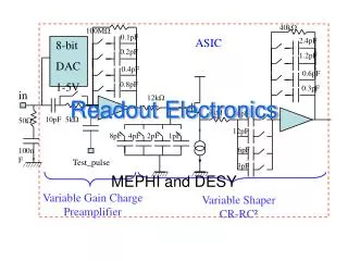
LAr TPC - Cold CMOS Electronics Block Diagram – Reference Design TIPP 2011 – Cold Electronics
LAr TPC Front-End ASIC • 16 channels • charge amplifier (adj. gain) • high-order filter (adj. time constant) • ac/dc, adjustable baseline • test capacitor, channel mask • ADC (12-bit, 2 MS/s) • compression, discrimination • multiplexing and digital buffering • LV or CM digital interface • pulse generator, analog monitor • temperature sensor • LAr environment (> 20 years at 88K) • estimated total size ~ 6 x 8 mm² • estimated power ~ 10 mW/channel
Analog ASIC • 16 channels • charge amplifier, high-order filter • adjustable gain: 4.7, 7.8, 14, 25 mV/fC • (charge 55, 100, 180, 300 fC) • adjustable filter time constant • (peaking time 0.5, 1, 2, 3 µs) • selectable collection/non-collection mode • (baseline 200, 800 mV) • selectable dc/ac coupling (100µs) • rail-to-rail analog signal processing • band-gap referenced biasing • temperature sensor (~ 3mV/°C) • 136 registers with digital interface • 5.5 mW/channel (input MOSFET 3.9 mW) • single MOSFET test structures • ~ 15,000 MOSFETs • designed for room (300K) and cryogenic (77K) operation • technology CMOS 0.18 µm, 1.8 V TIPP 2011 – Cold Electronics
Noise Measurements Layout Detail Qmax=300fC v1 v2 Input MOSFET L = 270 nm W = 10 mm (50µm x 200) gm,77K ≈ 90 mS (11 Ω) gm,300K ≈ 45 mS (22 Ω) Input Line L ≈ 1 mm W = 3.5 µm (M3 + M4) R77K ≈ 3 Ω R300K ≈ 12 Ω Dynamic Range > 3,000 • Measurements affected by: • input line parasitic resistance • ~ 150 e- at 77 K (~ 590 e- at 300K ) • addressed in next revision • CINdielectric noise (not present in wire) • ~ 60 e- at 77 K ASIC revision 2 designed and fabricated, currently being tested
FEE ASIC Evaluation FEE Test Stand for MicroBooNE is operational • Full front end electronics chain, from CMOS ASIC to Receiver/ADC board, data is acquired to PC through FPGA board and Gigabit Ethernet • One temporary 32 channel cold cable is available which has one broken channel • Without detector capacitance, noise is ~200e- with 1us peaking time • Nonlinearity and crosstalk are less than 0.5% • FEE test stand will be upgraded with the second version of ASICs and two prototype cold cables, more tests to follow TIPP 2011 – Cold Electronics
MOS Static Model IDvsVDS IDvsVGS Some differences in saturation voltage, sub-threshold slope, transconductance
Signal Measurements Bandgap Reference variation ≈ 1.8 % Temperature Sensor ~ 2.86 mV / °K Pole-zero cancellation at 77K to be addressed in next revision Adjustable gain, peaking time and baseline maximum charge 55, 100, 180, 300 fC
ADC - Architecture Clockless low power ADC stage Demonstrated in ASIC for SNS, see De Geronimo, et al., IEEE Trans NSS, 54 (2007) 541 • Current mode ADC • dual stage6-MSBs in 150ns, 6-LSBs in 250ns • single trigger conversion per stage • 12-bit resolution • 2 MS/s conversion rate • power dissipation 3.6 mW at 2 MS/s • power-down option for low rate applications • wake up in few tens of ns • layout size: 0.23 mm x 1.25 mm ADC cell
ADC - Preliminary Results 300 K 16-channel ADC+buffer 6mm 4.3 mm ADC output - 1.4 V sine ADC output - 500mV dc 77 K σ=1.1LSB • operation verified at room and cryogenic temperatures • differential non-linearity limited by timing design error in control circuit • integral non-linearity limited by mismatch (linear → common centroid) ASIC revision being designed, to be fabricated in July
Conclusions and Future Work • CMOS performs better at cryogenic temperatures • Defined and predictable design for cryogenic T is possible • Low-noise at cryogenic T demonstrated • ENC < 1,000 e- at 200pF ~5mW/ch. • characterization and modeling of CMOS 180nm • Long lifetime at cryogenic T possible with guidelines • Critical building blocks - front-end & ADC - developed • Future work • Improve cryogenic static models • Optimize ADC • Merge, add zero-suppression & buffering, and finalize June 11, 2011 TIPP 2011 – Cold Electronics
LAr TPC - Cold CMOS Electronics Block Diagram – Alernate Design June 11, 2011 TIPP 2011 – Cold Electronics
Calibration Scheme N1 = 20 N2 = 3, 5, 9, 16 CINJ = 180 fF nominal Integrated injection capacitance (10 x 18 µm²) Disabled (grounded) when unused change ~ 0.5% Measured with high-precision external capacitance
Lifetime - Basic Mechanism • Degradation is due to impact ionization • charge trap in oxide, interface generation → shift in Vth and gm • Substrate current is a monitor of impact ionization • increases with drain voltage • is higher in short channel devices • has a maximum at VGS≈ VDS/2 • increases as the temperature decreases J. Cressler et al. J. Cressler et al. Commercial technologies are rated 10 years lifetime (10% gm shift) in continuous ring oscillator operation: T = 300 K, L = Lmin, Vds = nominal VDD+5%, VGS≈ VDS/2)
Lifetime - Design Guidelines Accelerated tests at increased VDSallow extrapolation of lifetime Desired lifetimeat low temperature can be achieved by: 1. decreasing VDS (e.g. decreasing the supply voltage) 2. decreasing JD(i.e. decreasing the drain current density) 3. increasing L (i.e. non-minimum channel length devices) J. Cressler et al. Design guidelines can be obtained for: • digital circuits • - operate devices at -10% of nom. VDD • - use non-minimum channel length L • - operate at low clock frequency • analog circuits • - operate devices at low current density • - use non-minimum channel length L Accelerated tests at cryogenic temperature are being performed to verify guidelines