Download
1 / 13
130 likes | 309 Vues
Beams of Electrosprayed Nanodroplets for Surface Engineering. Manuel Gamero-Castaño Department of Mechanical and Aerospace Engineering University of California, Irvine. Energetic Impact by Electrosprayed Nanodroplets.

E N D
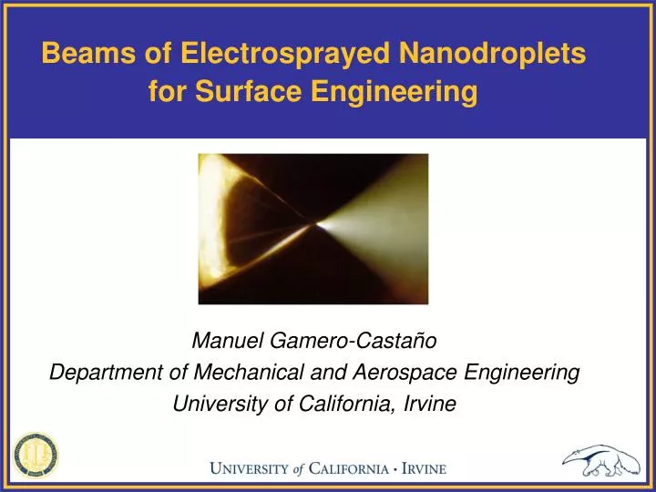
Beams of Electrosprayed Nanodroplets for Surface Engineering Manuel Gamero-Castaño Department of Mechanical and Aerospace Engineering University of California, Irvine
Energetic Impact by Electrosprayed Nanodroplets • Electrosprayednanodroplets fill the unexplored size range between ionic and macroscopic projectiles (between approx. 2-3 nm and 1 micron). Potential for new discoveries. • The impact of nanodroplets is similar to the hypervelocity impact of macroprojectiles. However local equilibrium is not reached near the impact, resulting in new and interesting phenomena. • Nanodroplets may extend the size-related advantages of cluster ion beams (low q/m → high molecular fluxes and sputtering rates, restricted damage depth, etc). • Unlike cluster ion beams, electrospraying is a point source and therefore its beam can be focused on a submicrometric spot (good for SIMS and micromachining applications).
How Do We Know the Droplet Size? • Extensive body of work on electrospraying in the cone-jet mode: accurate scaling laws for the droplet diameter and charge. • J. Fernández de la Mora, I.G. Loscertales, The current transmitted through an electrified conical meniscus. Journal of Fluid Mechanics 260,155-84 (1994). • F. J. Higuera, Flow rate and electric current emitted by a Taylor cone. Journal of Fluid Mechanics. 484, 303-327 (2003). • M. Gamero-Castaño, Energy Dissipation in Electrosprays and the Geometric Scaling of the Transition Region of Cone-Jets. Journal of Fluid Mechanics, 662, 493-513 (2010). • M. Gamero-Castaño, The Structure of Electrospray Beams in Vacuum. Journal of Fluid Mechanics, 604, 339-368 (2008). • Experimental determination of particle velocities and q/m via time-of-flight.
How Do We Know the Droplet Size? • Measuring an individual droplet’s charge and diameter via retarding potential analysis and induction charge detection in tandem. M. Gamero-Castaño, Retarding potential and induction charge detectors in tandem for measuring the charge and mass of nanodroplets, Rev. Sci. Instrum. 80, 053301 (2009). • Typical droplet and impact parameters (EMI-Im ionic liquid) Ie electrospray current; <q/m > average droplet charge to mass ratio; <D> av. droplet diameter; <Nm> av. number of molecules in droplet; <vd> av. droplet velocity; <Em> av. molecular energy; P projectile stagnation pressure; tPcharacteristic compression time
Sputtering of Si, SiC and B4C Experimental Setup M. Gamero-Castaño and M. Mahadevan, Sputtering Yields of Si, SiC and B4C under Nanodroplet Bombardment at Normal Incidence. Journal of Applied Physics, 106, 054305 (2009). M. Gamero-Castaño and M. Mahadevan, Sputtering of Silicon by a Beamlet of Electrosprayed Nanodroplets. Applied Surface Science. 255, 8556-8561 (2009).
Sputtering of Si, SiC and B4C Bombarded Si Wafer Photograph, profile and AFM image of a Si target bombarded for 15 minutes with a beamlet of EMI-Im nanodroplets at 14.1 kV acceleration voltage, and an electrospray current of 373 nA (34.8 nm average droplet diameter, 4.28 km/s impact velocity, 37.2 eV molecular kinetic energy)
Sputtering of Si, SiC and B4C Sputtering Yields and Sputtering Rates • The maximum sputtering yields for Si, SiC and B4C are 2.32, 1.48 and 2.29 atoms per molecule respectively. For a comparison with atomic ion beams, the sputtering yields of Si, SiC and B4C bombarded by Argon at normal incidence and 500 eV are 0.4, 0.8, and 0.2 atoms per ion. • The maximum nanodroplet sputtering rates for Si, SiC and B4C are 0.448, 0.172, and 0.170 mm/min. The associated current densities are 9.26x10⁻³, 1.55x10⁻² and 1.33x10⁻²mA/cm2 respectively. A broad-beam Ar source operates at a current density of 2 mA/cm2 and 500 V, and has sputtering rates of 0.060, 0.062, and 0.011 mm/min for Si, SiC and B4C. • A multiemitter electrospray source with a density of1600 emitter/cm2 would have a current density of the order of 0.4 mA/cm2;& its sputtering rate would be larger than that of a single emitter by a factor of the order of 40, and the overall improvement with respect to IBM would be between 120 and 600. & Luis F. Velásquez-García, Akintunde I. Akinwande, Manuel Martínez–Sánchez, “A Planar Array of Micro-Fabricated Electrospray Emitters for Thruster Applications”, Journal of Microelectromechanical Systems, 15, 1272-1280 (2006)
Surface Morphology and Sputtering Yield at Increasing Impact Energy Si targets bombarded at increasing acceleration voltage Sputtering yield as a function of acceleration voltage 9.5 kV 11.0 kV 14.0 kV 12.5 kV 15.5 kV 17.5 kV
EBSD & HRTEM Confirmation of Amorphous Si Layer High resolution transmission electron microscopy image Electron backscatter diffraction mappings of bombarded surface b a-Si Si IPF colouring Z0
Pressure-Induced Amorphization Resulting from the Absence of Local Equilibrium • No amorphization has ever been observed in macroscopic shock compression of Si. The recovered material is always in the low pressure, cubic diamond crystalline phase. • Si undergoes a high pressure crystalline phase transition at about 12 GPa, evolving from the cubic diamond to the metallic b-Sn phase. The transition is reconstructive and has sluggish kinetics. • A likely explanation for the observed amorphization is that the nanodroplet impact compresses the cubic diamond phase beyond its thermodynamic stability domain, but the brief compression time impedes the growth of the b-Snphase. The cubic diamond lattice progressively deforms without being able to transform to the b-Snphase, and eventually loses its long-range order becoming amorphous.
Amorphous Surface May Have Improved Wear Properties Nanodroplet impact on crystalline vs. amorphous surface The absence of dislocations and grain boundaries in the amorphous phase impede the propagation of cracks and the fragmentation of the material
Future Work • Study the bombardment of colloid thrusters’ extracting electrodes by energetic nanodroplets and molecular ions. • Study whether the observed amorphization of Si is reproduced on other crystalline materials undergoing high pressure, reconstructive, crystalline phase transitions (e.g. Ge, SiC, GaAs, GaP, GaSb, InAs, InP, etc). New general, pressure-induced amorphization method. • Study of single nanodroplet impact, using RPA-ICD detector to characterize projectile on its way to a target. • Multi-scale modeling, first-principles understanding of the impact. • 3-D molecular profiling of organic surfaces via SIMS.