Download
1 / 48
480 likes | 613 Vues
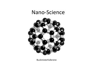
PREAMBLE OF NANO SCIENCE. PREAMBLE STRUCTURE HOLLISTIC FIX KEY CONCEPT KEY RESEARCH AREA KEY APPLICATION INDUSTRIAL APPLICATION RESEARCH HOW WE STUDY KEY JOBS PROJECTS ONE CAN DO TRENDS. INDEX. NAME OF THE INSTRUCTOR Ashish Kumar Singh 2. CABIN LOCATION

E N D
PREAMBLE STRUCTURE • HOLLISTIC FIX • KEY CONCEPT • KEY RESEARCH AREA • KEY APPLICATION • INDUSTRIAL APPLICATION • RESEARCH • HOW WE STUDY • KEY JOBS • PROJECTS ONE CAN DO • TRENDS INDEX
NAME OF THE INSTRUCTOR Ashish Kumar Singh 2. CABIN LOCATION Room No: 435 3. TELEPHONENO. 9808176088 4. EMAIL-ID: ashish.nmpt@gmail.com 5. MEETING HOURS– Faculty should provide 1 hour on all week days preferably between extended lunch break. ( 1.30 pm to 2.30 pm) TEACHERS INTRODUCTION
PREREQUISITES • Basic Knowledge of sciences (Before 12th standard) • (12th standard) • Basic Knowledge of Physics. • Basic Knowledge of Maths. • Basic Knowledge of Chemistry. HOLLISTIC FIX OF DIGITAL COMMUNICATION
HOLLISTIC FIX………Continued • Engineering mathematics • Calculus- Integral and differential • Environmental Sciences • Hydro Electric, Fossil Fuel based, Nuclear, Solar, Biomass and Bio-gas. And Hydrogen Energy. • Environmental Pollution and their effects. • Engineering Chemistry • Chemical reactions • Chemical bonding • PRE REQUISTES • (1st Semester) • Basic Principles of LASER • Introduction to optics • Interference • Diffraction • Polarization • Basics of Optical fibers • Types of optical fibers • Communication in optical fiber • loss and Attenuation
HOLLISTIC FIX………Continued • Electrical engineering • Current and Voltage • Electrical devices • Electronics engineering • Semiconductor physics • Electronic Instruments • Manufacturing processes • Properties of materials • Ferrous and Non- ferrous materials • PRE REQUISTES • (2nd Semester) • Basic Principles of Nano Science • Introduction to Quantum mechanics • Wave particle duality • Uncertainty Principal • Wave functions • Schrödinger wave equations • Electromagnetic waves • Propagation mechanism of EMW. • Pointing vector 6
ADVANCE COURSE (6th-7th SEM) • VLSI technology and Design • Analog Integrated electronics • Optical Fiber Communication • Power electronics (8th SEM) • Optical fiber communication • Electrical instrumentation and process control HOLLISTIC FIX OF DC………Continued
SCOPE IN RELATED FIELDS… • Mobile Communication • Wireless Technologies- • Microprocessors • Integrated Circuits • Aerospace • Solar cell HOLLISTIC FIX OF DC…….Continued http://research.nokia.com/files/PIMRC07-1169.pdf- wirless technology http://www.inemi.org/- nano technology + electronics
10 What is Nanoscale Science? • The study of objects and phenomena at a very small scale, roughly 1 to 100 nanometers (nm) • 10 hydrogen atoms lined up measure about 1 nm • A grain of sand is 1 million nm, or 1 millimeter, wide • An emerging, interdisciplinary science involving • Physics • Chemistry • Biology • Engineering • Materials Science • Computer Science Source: http://www.cs.utexas.edu/users/s2s/latest/bialt1/src/WhatIsNano/images/molecule.gif
11 How Big is a Nanometer? • Consider a human hand skin white blood cell DNA atoms nanoscale Source: http://www.materialsworld.net/nclt/docs/Introduction%20to%20Nano%201-18-05.pdf
Are You a Nanobit Curious? • What’s interesting about the nanoscale? • Nanosized particles exhibit different properties than larger particles of the same substance • As we study phenomena at this scale we… • Learn more about the nature of matter • Develop new theories • Discover new questions and answers in many areas, including health care, energy, and technology • Figure out how to make new products and technologies that can improve people’s lives
So now that we can “see” what’s going on… How do properties change at the nanoscale? Size-Dependent Properties
Properties of a Material • A property describes how a material acts under certain conditions • Types of properties • Optical (e.g. color, transparency) • Electrical (e.g. conductivity) • Physical (e.g. hardness, melting point) • Chemical (e.g. reactivity, reaction rates) • Properties are usually measured by looking at large (~1023) aggregations of atoms or molecules Sources: http://www.bc.pitt.edu/prism/prism-logo.gif http://www.physics.umd.edu/lecdem/outreach/QOTW/pics/k3-06.gif
Optical Properties Change: Color of Gold • Bulk gold appears yellow in color • Nanosized gold appears red in color • The particles are so small that electrons are not free to move about as in bulk gold • Because this movement is restricted, the particles react differently with light 12 nanometer gold clusters of particles look red “Bulk” gold looks yellow Sources: http://www.sharps-jewellers.co.uk/rings/images/bien-hccncsq5.jpg http://www.foresight.org/Conferences/MNT7/Abstracts/Levi/
Electrical Properties Change: Conductivity of Nanotubes • Nanotubes are long, thin cylinders of carbon • They are 100 times stronger than steel, very flexible, and have unique electrical properties • Their electrical properties change with diameter, “twist”, and number of walls • They can be either conducting or semi-conducting in their electrical behavior Electric current varies by tube structure Multi-walled Source: http://www.weizmann.ac.il/chemphys/kral/nano2.jpg
Physical Properties Change:Melting Point of a Substance • Melting Point (Microscopic Definition) • Temperature at which the atoms, ions, or molecules in a substance have enough energy to overcome the intermolecular forces that hold the them in a “fixed” position in a solid • Surface atoms require less energy to move because they are in contact with fewer atoms of the substance In contact with 3 atoms In contact with 7 atoms Sources: http://puffernet.tripod.com/thermometer.jpg and image adapted from http://serc.carleton.edu/usingdata/nasaimages/index4.html
Size Dependant Properties Why do properties change?
Scale Changes Everything • There are enormous scale differences in our universe! • At different scales • Different forces dominate • Different models better explain phenomena • (See the Scale Diagram handout)
Scale Changes Everything II • Four important ways in which nanoscale materials may differ from macroscale materials • Gravitational forces become negligible and electromagnetic forces dominate • Quantum mechanics is the model used to describe motion and energy instead of the classical mechanics model • Greater surface to volume ratios • Random molecular motion becomes more important
Dominance of Electromagnetic Forces • Because the mass of nanoscale objects is so small, gravity becomes negligible • Gravitational force is a function of mass and distance and is weak between (low-mass) nanosized particles • Electromagnetic force is a function of charge and distance is not affected by mass, so it can be very strong even when we have nanosized particles • The electromagnetic force between two protons is 1036 times stronger than the gravitational force! Sources: http://www.physics.hku.hk/~nature/CD/regular_e/lectures/images/chap04/newtonlaw.jpg http://www.antonine-education.co.uk/Physics_AS/Module_1/Topic_5/em_force.jpg
Quantum Effects • Classical mechanical models that we use to understand matter at the macroscale break down for… • The very small (nanoscale) • The very fast (near the speed of light) • Quantum mechanics better describes phenomena that classical physics cannot, like… • The colors of nanogold • The probability (instead of certainty) of where an electron will be found Macrogold Nanogold Sources: http://www.phys.ufl.edu/~tschoy/photos/CherryBlossom/CherryBlossom.html http://www.nbi.dk/~pmhansen/gold_trap.ht; http://www.sharps-jewellers.co.uk/rings/images/bien-hccncsq5.jpg;
Surface to Volume Ratio Increases • As surface to volume ratio increases • A greater amount of a substance comes in contact with surrounding material • This results in better catalysts, since a greater proportion ofthe material is exposed for potential reaction Source: http://www.uwgb.edu/dutchs/GRAPHIC0/GEOMORPH/SurfaceVol0.gif
Random Molecular Motion is Significant • Tiny particles (like dust) move about randomly • At the macroscale, we barely see movement, or why it moves • At the nanoscale, the particle is moving wildly, batted about by smaller particles • Analogy • Imagine a huge (10 meter) balloon being batted about by the crowd in a stadium. From an airplane, you barely see movement or people hitting it; close up you see the balloon moving wildly. Source: http://www.ap.stmarys.ca/demos/content/thermodynamics/brownian_motion/rand_path.gif
Potential Impacts How might nanoscale science and engineering improve our lives?
Innovations In Development or Under Investigation • Health Care • Chemical and biological sensors, drugs and delivery devices, prosthetics and biosensors • Technology • Better data storage and computation • Environment • Clean energy, clean air Thin layers of gold are used in tiny medical devices Carbon nanotubes can be used for H fuel storage Possible entry point for nanomedical device
Health Care: Nerve Tissue Talking to Computers • Neuro-electronic networks interface nerve cells with semiconductors • Possible applications in brain research, neurocomputation, prosthetics, biosensors Snail neuron grown on a chip that records the neuron’s activity Source: http://www.biochem.mpg.de/mnphys/publications/05voefro/abstract.html
Technology: A DVD That Could Hold a Million Movies • Current CD and DVD media have storage scale in micrometers • New nanomedia (made when gold self-assembles into strips on silicon) has a storage scale in nanometers • That is 1,000 times more storage along each dimension (length, width)… …or 1,000,000 times greater storage density in total! Source: Images adapted from http://uw.physics.wisc.edu/~himpsel/nano.html
Technology: Building Smaller Devices and Chips • Nanolithography to create tiny patterns • Lay down “ink” atom by atom Transporting molecules to a surface by dip-pen nanolithography Mona Lisa, 8 microns tall, created by AFM nanolithography Sources: http://www.ntmdt.ru/SPM-Techniques/Principles/Lithographies/AFM_Oxidation_Lithography_mode37.html http://www.chem.northwestern.edu/~mkngrp/dpn.htm
Environment: Nano Solar Cells • Nano solar cells mixed in plastic could be painted on buses, roofs, and clothing • Solar becomes a cheap energy alternative! ] 200 nm Nano solar cell: Inorganic nanorods embedded in semiconducting polymer, sandwiched between two electrodes Source: http://www.berkeley.edu/news/media/releases/2002/03/28_solar.html
So How Did We Get Here? New Tools! As tools change, what we can see and do changes
Using Light to See • The naked eye can see to about 20 microns • A human hair is about 50-100 microns thick • Light microscopes let us see to about 1 micron • Bounce light off of surfaces to create images to see red blood cells (400x) Light microscope (magnification up to 1000x) Sources: http://www.cambridge.edu.au/education/PracticeITBook2/Microscope.jpg http://news.bbc.co.uk/olmedia/760000/images/_764022_red_blood_cells300.jpg
Using Electrons to See • Scanningelectron microscopes (SEMs), invented in the 1930s, let us see objects as small as 10 nanometers • Bounce electrons off of surfaces to create images • Higher resolution due to small size of electrons (4000x) Greater resolution to see things like blood cells in greater detail Sources: http://www.biotech.iastate.edu/facilities/BMF/images/SEMFaye1.jpg http://cgee.hamline.edu/see/questions/dp_cycles/cycles_bloodcells_bw.jpg
Touching the Surface • Scanning probe microscopes, developed in the 1980s, give us a new way to “see” at the nanoscale • We can now image really smallthings, like atoms, and move them too! This is about how big atoms are compared with the tip of the microscope Source: Scientific American, Sept. 2001
Nanotechnology is a Frontier in Modern-Day Science What else could we possibly develop? What other things are nanoengineers, researchers and scientists investigating?
Detecting Diseases Earlier • Quantum dots glow in UV light • Injected in mice, collect in tumors • Could locate as few as 10 to 100 cancer cells Quantum Dots: Nanometer-sized crystals that contain free electrons and emit photons when submitted to UV light Early tumor detection, studied in mice Sources: http://vortex.tn.tudelft.nl/grkouwen/qdotsite.html http://www.whitaker.org/news/nie2.html
Growing Tissue to Repair Hearts • Growing cardiac muscle tissue is an area of current research • Grown in the lab now, but the fibers grow in random directions • With the help of nanofiber filaments, it grows in an orderly way • Could be used to replace worn out or damaged heart tissue Cardiac tissue grown with the help of nanofiber filaments Source: http://www.washington.edu/admin/finmgmt/annrpt/mcdevitt.htm
Preventing Viruses from Infecting Us • The proteins on viruses bind to our body cells • Could cover these proteins with nanocoatings • Stop them from recognizing and binding to our cells • We would never get the flu! • A protein recognition system has been developed Influenza virus: Note proteins on outside that bind to cells Gold tethered to the protein shell of a virus Sources: http://www.zephyr.dti.ne.jp/~john8tam/main/Library/influenza_site/influenza_virus.jpg http://pubs.acs.org/cen/topstory/8005/8005notw2.html
Making Repairs to the Body • Nanorobots are imaginary, but nanosized delivery systems could… • Break apart kidney stones, clear plaque from blood vessels, ferry drugs to tumor cells Source: http://www.genomenewsnetwork.org/articles/2004/08/19/nanorobots.php
Research areas in cluster of DC: • Fast Multiple Access more than the speed of light. • To reduce the complexity & cost of Receiver & Transmitter used in DC components. • To reduce the noise to a zero level • Efficient long range communications • To increase the Channel Capacity KEY RESEARCH AREA OF DIGITAL COMMUNICATION
Key Jobs & Companies http://www.workingin-nanotechnology.com/ www.nano.gov/nni_energy_rpt.pdf http://www.nano.gov/html/research/home_research.html http://research.nokia.com/projects/nanosciences http://www.nsf.gov/news/overviews/nano/screensaver.jsp http://www.nanotech-now.com/business.htm
CSIR- India. http://www.csir.res.in/ Bhabha atomic and Research Center. http://www.barc.ernet.in/ Hindustan Aeronautics Limited. www.hal-india.com Defense Research & Development Organization. www.drdo.org Indian space research organization. http://www.isro.org/ PUBLIC SECTOR JOBS
Nanotechnology Applications • Remediation • Sensors • Treatment • Green Manufacturing • Green Energy • Nanotechnology Implications • Aerosol • Life Cycle Assessment • Industrial Ecology • Toxicity • Fate and transport • Exposure • STAR Awards by RFA • SBIR Nano Research • Ultrafine Particle Research Projects in nanoscience