Download
1 / 72
730 likes | 840 Vues
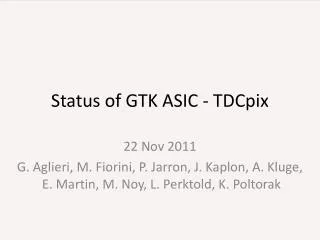
Status of GTK ASIC - TDCpix. 22 Nov 2011 G. Aglieri, M. Fiorini, P. Jarron, J. Kaplon, A. Kluge, E. Martin, M. Noy, L. Perktold, K. Poltorak. TDCpix ASIC block diagram (60 bit serial/5 LVDS pairs parallel). 45. 2011.10.24. 4x45. 45. 2.7 /4 Mhits/s. Config pixel. 5 bit trimDAC.

E N D
Status of GTK ASIC - TDCpix 22 Nov 2011 G. Aglieri, M. Fiorini, P. Jarron, J. Kaplon, A. Kluge, E. Martin, M. Noy, L. Perktold, K. Poltorak
TDCpix ASIC block diagram (60 bit serial/5 LVDS pairs parallel) 45 2011.10.24 4x45 45 2.7 /4 Mhits/s Config pixel 5 bittrimDAC pixel driver&line&receiver pixel cell x 45 pixel column double column 0 column 1 double column 5 double column 4 double column 3 double column 1 double column 6 double column 2 double column 19 end of column 5 2, parallel_load&daq_rdy hitArbiter 0 & edge detector hA 1 hA 8 hA 2 column 0 1,hit 32 clkdll=320MHz coarseTimeStamp DLL fineHitRegister0 coarseHitRegister0 DLL 0 2 x 32 2 x (13 + 5) 5 add+5 pil serialTime state machine 12 1 > CP&PD clksync or clkserialTime syncRegister 2 x 32 2 x (13 + 5) 5 add+5 pil clkdll coarseTimeStampServer0 > 9 fineTimeStampEncoder coarseTimeStampEncoder group EOC 1 group EOC 2 group EOC 8 group EOC 0 5 rise+5 trail 13 rise+5 trail 5 address + 5 pileup 32 fineRise 32 fineTrail 2x12+1 coarseRise 2x4+1 coarseTrail 5 fineRise 5 fineTrail 12+1 coarseRise6+1coarseTrail 2 group collision > clksync 0.3/0.44 Mhit/s pixelGroupFifo(depth= 3) 648 FF @ 2 depth 8 bit thresholdDACcolumn & 3 bit bias DAC 42 42 5 rise+5trail+12+1 rise+6+1 trail+5add+5pil+2col=42 42 columnMux 9 to 1 23 cell units * (0.40 µmx 4.8 µm)* (648+152+373/10) FF=37000 µm2=124µm*300µm ConfigDoubleCol 42+4 add=46 2.7/ 4 Mhit/s columnFifo (depth= 6) columnFifoController clksync > 152FF @ 4 depth 5x doubleCol x 2x42+2x9 42 46 serialTime 1 column 9 columns quarterchipFifo&frameInserter Controller > clksync & enableclk sync register 90 clksync serialTime Controller quarterChipMux 10 to 1 serialTimeMux 90 to 48 > clksync clksync 48 46+4 add=50 quarter chip RO 0 Full FIFO info column: ((occupancy 2, overflow count 3)*9+2+1,8)*2.5= quarterChip: occupancy 3+1, overflow count 8=12 quarter chip RO 3 quarter chip RO 2 quarter chip RO 1 data formatter & multipleHit & comma & frame inserter 48 min. 40 FIFOs 1 FIFO overflow bit, optional overflow count > > clksync & enableclk clksync & enableclk 8b10b encoder sync register 60 > > clkserial/2 serializer controller clkserial/2 clkmultiserial 27/ 40 Mhit/s parallelOut > 2 58 0 clkserial/2 (enable)/ mode serializer FIFO overflow status > 3 59 1 2.4/3.2 Gbits/s CML driver multiSerialPower 4 x LVDS480/640 Mbit/s clkmultiserial path d is doubled as to have one direct link from clkserial/2 to clkfiforead clkFIFOread 2 world clkserial/2 clksync 1 clkmultiserial or clktest CMOS DC global DACs clkSerial=2.4/ 3.2 GHz c Modes: serialPLL2.4/serialPLL3.2/ext320/ext480/PLLoverride abc: 0000/0000/111*1/110*1/100*1 8 modes = 3 bits clkInDigital=20/26.66/320/480/320MHz clkPLL=2.4/3.2/-/-/0.32GHz clksync=240(10)/ 320(10)/ 320*(1)/240*(2)/32(1) MHz clkFIFOread=40(60)/53(60)/27(12)/40(12)/5.3 MHz(60) clkmultiserial=480/640/320/480/64 MHz clkserialtime=clksync () =division factor, * can also be 0 or 1 to change clksync in TDC /2 /2 /5 /6 1 0 0 PLL 9+1x temp 1 /5 reset_corsecnt LVDS reset_global CMOS 0 1 PLL override reset_dll CMOS bandgap override 1 0 ext a b c d config/statuschip band gap 2 (1 temp) test pulse analogMonitorMux b d clkDigital=20/26.7 MHz muxmode LVDS320 MHz PLL qchip clock divider & clk distribution LVDS≥320 Mbit/s diffanalog AC 3 clkDll analog DC LVDS 320/480MHz CMOS DC is located in synchronous logic; clk divider needs synchronous reset with respect to receiving clock domain (clkmultiserial) avg. nominal rate (750 MHz beam (104 Mhit/s per chip) / rate with 2.4 Gbiit/s serializer [Mhit/s]) = SEU protected
2011.10.24 enable/clkFIFOread clksyncReg /nonext clkserial/2 clksync clkmultiserial /6 clkserialTime clksync clkserialTime /ext clkSerial=2.4/3.2 GHz /10 /ext PLL /60 or ext/12 /2 /5 /5 or ext PLL override /10 or ext/2 ext /2 muxmode clkDigital=20/26.7 MHz 2 PLL & clock divider & clk distribution LVDS 320/480MHz CMOS DC clkmultiserial path d is doubled, but mux d and div 6 will be sitting in serializer to keep routing short. clkFIFOread clkserial/2 clksync Modes: serialPLL2.4/serialPLL3.2/ext320/ext480/PLLoverride abc: 0000/0000/111*1/110*1/100*1 8 modes = 3 bits clkInDigital=20/26.66/320/480/320MHz clkPLL=2.4/3.2/-/-/0.32GHz clksync=240(10)/ 320(10)/ 320*(1)/240*(2)/32(1) MHz clkFIFOread=40(60)/53(60)/27(12)/40(12)/5.3 MHz(60) clkmultiserial=480/640/320/480/64 MHz clkserialtime=clksync () =division factor, * can also be 0 or 1 to change clksync in TDC clkSerial=2.4/ 3.2 GHz c /5 /6 /2 /2 /5 1 0 0 PLL 1 1 0 PLL override 1 0 ext a b c d b d clkDigital=20/26.7 MHz muxmode 3 PLL & clock divider & clk distribution LVDS 320/480MHz CMOS DC is located in synchronous logic; clk divider needs synchronous reset with respect to receiving clock domain (clkmultiserial) avg. nominal rate (750 MHz beam (104 Mhit/s per chip) / rate with 2.4 Gbiit/s serializer [Mhit/s])
12000 µm Column 0 Corners: 125 µm Pixel = column * 45 + row Pixel group = column * 9+ group group 0 contains pixel 0 Pixel matrix: 13500 µm row 0 EoColumn bias 1800 µm TL rx: 70 µm hitArbiter 175 µm DLL, SM, fine registers 1000 µm Band Gap 250x1000 Aux. components 500x250 Test pads 250x1500 Coarse units, pixel group FIFOs, column FIFO 1075 µm Routing adaptor 1000x200 qchipRo1 2500x1000 qchipRo0 2500x1000 qchipRo3 2500x1000 Quarter chip read-out & Global configuration ~ 1000 µm qchipRo2 2500x1000 chipConfig 1000x600 Serializer1 2000x500 Serializer0 2000x500 Serializer3 2000x500 Serializer2 2000x500 PLL&clock 1000x500 Serializer & PLL & clock distributor ~ 500 µm Pad ring 12000 x 700 Pad ring ~700 µm Total: 19945 µm
min: clk_prop + hold; max: clk_prop+clk_cycle-setup cmd_reset_bandgap reset_bandgap_n from outside and analog blocks low active reset digital logic high active reset reset_synchronizer_sync D D D D D D D D D Q Q Q Q Q Q Q Q Q _ _ _ _ _ _ _ _ _ Q Q Q Q Q Q Q Q Q clk_sync clk_sync clk_sync cmd_reset_sync cmd_reset_dll clk_dll cmd_config clk_config *) pin reset_all_n reset_sync, reset_dll, reset_config, reset_bandgap_n *) cmd_reset_all reset_sync, reset_dll, reset_config, reset_bandgap_n *) cmd_reset_sync reset_sync *) cmd_reset_dll reset_dll (to dll_state_machine) *) cmd_reset_config reset_config *) cmd_reset_bandgap reset_bandgap_n Reset scheme
Data format • Nominal transmission: 2.4 Gbits/s, • High speed: 3.2 Gbits/s • All words: 48 bits (6 bytes) long • 8b10 encoded bit stream 60 bits • data word • frame word • idle (komma) word: no hits available to transmit, 6 * comma character (ie. K28.5) • sync word: after reset and after each force_sync command (can be sent repetitive)for 4 * 106 cycles, 100 ms @ 2.4 Gbit/s, 6 * comma character (ie. K27.7) • link checking sequence, known pattern (ie. counter) sent upon request • Header contains frame counter every 6.4 µs • Data contains dynamic range up to 6.4 µs + 1 overroll counter bit
Data format-hit word normal mode (48 bit) • ------------------------------------------------------------------ • --qchip_word -> data_out • ------------------------------------------------------------------ • --(47) Status/data selector 1 bit • --(46..40) Address 7 bit (90 pixel groups) • --(39..35) Address-hit arbiter 5 bit • --(34..30) Address pileup 5 bit • --(29) Leading coarse time selector 1 bit • --(28..17) Leading coarse time 12 bit 1bit rollover indicator+2048(11bit)*3.125 ns=6.4 µs • --(16..12) Leading fine time 5 bit 98 ps -> 3.125 ns • --(11) Trailing coarse time selector 1 bit • --(10..5) Trailing coarse time 6bit 64*3.125 ns = 200 ns • --(4..0) Trailing fine time 5 bit 98 ps -> 3.125 ns • ___________________________________________________________ • --Total 48 bit
(45..39) Address 7 bit (90 pixel groups) • 10 column each 9 pixels groups to be addressed: • Column 0: pixel group 0,1,2,3,…,7,8 • Column 1: pixel group 9,10,11,12,13..17 • Column 2: pixel group 18,19,20,21,..26 • …. • pixels in pixel group are one hot encoded • example pixel 2: “00010”
Data format-status words • ------------------------------------------------------------------ • -- word_frame0 • ------------------------------------------------------------------ • --(47) status bit 1 bit • --(46..41) # of SEU in previous frame 6 bits 2**6=64, 64/6.4us=10E7/s • --(40..28) # of hits in previous frame 13 bits 2*1*3=8192, hits per qchip and frame= 130 Mhits/s/4*6.4us=208->factor 40 --> 2048 --> 13 bit • --(27..0) framecounter 28 bit 2**28*6.4us=1718s • ___________________________________________________________ 48 bit • -- word_frame1 • --(47) status bit 1 bit • --(46..31) checksum 16 bit • --(31..6) empty 26 bit • --(5..0) group collision count 6 bit • ___________________________________________________________ • -- 48 bit
sync link word (48 bit) sent after reset for 1024 clk cycles • 6 * Komma K28.5___________________________________________________________________________________ • Total 6 * 48bit
sync slot word (48 bit) sent after sync link word for 1024 clk cycles • 5 * Komma K27.7+ 1 D0.0 + D0.0 is sent after 5 Kommas___________________________________________________________________________________ • Total 6 * 48bit
idle word (48 bit) • 6 * Komma K27.7___________________________________________________________________________________ • Total 6 * 48bit
Do we need these values in frame • Seu_counter • FIFO_overflow_counter • Error_info • Status_info • Checksum
Configuration: qChip • --(0) 1 bit: send_k_sync_requ • --(1) 1 bit: send_k_word_requ • --(5.2) 2 bit: k_word_type • --(6) 1 bit: send_testpattern_requ • --(14..7) 8 bit: • rotating FIFO 48 bits * 8 words • --> subsequentwriting moves write pointer of FIFO sothatall FIFO cellscanbewritten • --> when test pattern FIFO is used, all 8 FIFO cells are read and pushed into • --> the data stream, thus the data stream consists of a multiple of 8 data words. • --(15) 1 bit: new_data_testpattern • --(..16) serial read-out control • --send_k_sync_requ <= configuration_data_in(0); • --send_k_word_requ <= configuration_data_in(1); • --k_word_type <= configuration_data_in(5 downto 2); • --send_testpattern_requ <= configuration_data_in(6); • --data_testpattern <= configuration_data_in(14 downto 7); • --new_data_testpattern <= configuration_data_in(15); • --serial read-out control <= ….
Data format-hit word extended mode, not implemented • Status/data selector 1 bit • Leading coarse time 12 bit 2048*3.125 ns=6.4 µs • Leading fine time 5 bit 98 ps -> 3.125 ns • 2x Trailing coarse time 2x5 bit 32*3.125 ns = 100 ns • 2x Trailing fine time 2x5 bit 98 ps -> 3.125 ns • Coarse time selector 2 bit • Address 12 bit • Address-hit arbiter 5 bit (3 bit possible, but loss if double address bit info) • Address-pixel group 7bit (9 x 10 pixel groups in quarter chip -> encoding required) • Address pileup 5bit(can be encoded into if only one pileup info sufficient or can be sent as second word) • Error bit (SEU, overflow) 2 bit bit (can be sent afterwards as status word)___________________________________________________________________________________ • Total 59 bit sent in two 48 bits words
Status • schematic or hdl • simulation pre-layout / pre-synthesis • layout & extraction • simulation post-layout / parasitics back annotated • DRC & LVS • schematic integrated in top • layout integrated in top • simulation integrated in top • SEU simulation
Implementation data transmission 60b • Using GBT running at 20 MHz, but modifying data shift length to 60 • Problem: GBT has 3 parallel multiplexed shift registers, 60/3=20GBT can to be modified to 2 SR each 30 bits, first clock divider from 3 to 2additional high speed dividers • 20 MHz in 2.4 Gbit/s 40 Mwords/s (+21% (132 Mhits/s); + 54% (104 Mhits/s) • 2400 / 320 = 7.5 ! 2400/8 = 300 MHz • Programmable divider: 10 (240) / 5! (480) / 60 (40) for synchronous read logic • Programmable divider: 8 (300), 6(400) for FIFO write and state machines • Synchronous parallel read-FIFO frequency: • serialFrequ * n / 50 [MHz] = 48 (1)/96(2)/144(3)/192/240(10)/288/336/384/432/480 (5!) 20 MHz 2.4 GHz PLL • Fast counter: • /2 = 1.2 GHz serial mux & shift • /5 /2 = 240 MHz fifo read • /5/2 = 240; /2 /4 = 300 MHz; /3 /2 = 400 MHzstatemachines, all FIFOs&chipFIFOwrite 1.2 GHz serial mux & shift 40 MHz parallel_load (/60) Clock divider 2.4 GHz 40 MHz (60) / 240 MHz (10) / 480 MHz (5!) Fifo read 240 MHz (10) / 300 MHz (8) / 400 (6) Fifo write
Implementation data transmission; 60bit/5IO • Multi Serial60bit: • 60 bits (8b10); 5 I/O pairs • FIFO read-frequency for 50% contingency on 132 Mhits/s 50 MHz / quarter chip * 60 bit /5 pairs (10 bits serializer) 3000 /5 = 600 MHz per LVDS pair • Input frequency comes from PLL or from outside, either 2.4 Gbit/s on pad or 480 MHz for all pads & synchronous logic • if synchronous logic works with 480 MHz only 480 MHz * 5 = 2400 Mbit/s / 60 40 Mhits/s (21 % (132 Mhits/s) +54 % (104 Mhit/s)) • Worst case • synchronous logic works with 320 MHz only 320 MHz * 5 = 1600 Mbit/s / 60 26.7 Mhits/s (-19 % (132 Mhits/s) +3 % (104 Mhit/s)) • synchronous logic works with 240 MHz only 240MHz * 5 = 1200 Mbit/s / 60 20 Mhits/s (-39 % (132 Mhits/s) -23 % (104 Mhit/s))
Implementation data transmission 60b • Using GBT running at 26.66 MHz • 26.66 MHz in 3.2 Gbit/s 53 Mwords/s (+61 % (132 Mhits/s); + 105 % (104 Mhits/s) • 3200 / 320 = 10 • Programmable divider: 10 (320) 26.66 MHz 3.2 GHz PLL 3.2 GHz 53MHz parallel_load (/60) Clock divider 3.2 GHz 53 MHz (60) / 320 MHz (10) / 640MHz (5!) Fifo read 320MHz (10) / 400 MHz (8) / 533.33 (6) Fifo write
IOs • south end of chip: • 12 mm-2 corners*0.215 mm / 0.073 mm pitch = 158 • if possible only one rowoptional, two rows with power pins in the 2nd row (longer bond wires) • bond pads 200 µm long x ~ 70 µm wide • east and west end: • area accessible when sensor bonded: x mm pads • area not accessible when sensor bonded: x mm pads available for test pads in the EOC area
Which test pads for building blocks? • TDC inputs. • Can they be put in 2nd row? or on the side? • How much space for EOC? 4.5mm+padrow=5 mm • How much space of ASIC not under sensorminus corner / 73µm *2 is # test pads
Test pads • divided PLL output on test pad
Chip assembly • Global floor planning • Placement of pixel matrix, TDC, EOC, pad ring, configuration, auxiliary blocks • Power routing • Global functionality simulation • DRC, LVS • Top level schematic • Chips size compatibility with sensor, dicing, bump bonding
Block assembly • Pixel matrix (Virtuoso) • Pixel cell, inPixelconfinguration, inpixel DACs • EOC blocks (Encounter) • TDC, hitArbiter, FIFOreadout, quadConfiguration, chipConfiguration • Global blocks (Virtusoso/Encounter, depending on competency) • Serializer, IO ring, band gap, temperature
Verification sequence • Test patterns • From hit generator or • From configuration pattern • Individual blocks • Behavioral/functional • Layout DRC/LVS • Timing back annotated, worst/best case (libraries) • Local top level (ie. TDC, FIFOread-out, full configuration • Full functional back annotated with test patterns • Global top level (pixel matrix&digital&serializer) • Full functional back annotated (digital) with test patterns&simulated configuration & HDL modeled analog front-end & HDL modeled DLL • Functional simulation • SEU simulation • Mixed mode simulation on interface: transmission line & receiver & hitArbiter • DRC/LVS, (if possible full chip) • Global system test bench (pattern generator, verification of data output, assertions)
Pixel cell & matrix • Pixel cell • Pre-amplifier, discriminator, transmission line driver • In pixel DAC • In pixel configuration • Qualification • analog: extraction, connectivity, crosstalk sensitivity • config: functionality, connectivity • Pixel matrix • Top level schematic • column layout • transmission lines • Transmission line receiver • placement • Translation to 1.7 OA • Qualification • extraction, simulation • power routing • test pulse routing • biasing DACs • bias routing • configuration routing • Bias monitoring & mux • Qualification • analog: extraction, connectivity, crosstalk sensitivity, power drop • config: functionality, connectivity
Pixel cell & matrix • Analog End-of-column • Column DAC • Column DAC control • Temperature/radiation diodes • ADC • direct output
TDC • Delay line • Delay line, charge pump, loop filter • State machine • Qualification • DLL, operation margins, startup, extraction • Top level, including state machine
TDC • TDC • Floorplanning • Delay line • 32-5 encoder • synthesis, layout, simulation • fine hit registers • Layout, simulation, qualification with routing effects • course counter • concept • synthesis • qualification • hit arbiters & edge detector • schematic, simulation, layout • Qualification • State machine • placement, routing, Interconnection bus • Verification of power consumption • power routing TDC & compatibility with pixel matrix/global power routing • Qualification • extraction, functionality, crosstalk, power routing, top level, mixed mode • Top level schematics • Functional simulation (startup & time tag) • Timing simulation with hitArbiterController & FIFO controller & serial read-out controller
HitArbiter • Test bench • Remove demonstrator problems • Double hits, varying delays, pileUp address • Move to OA , 1.7 • Simulate backannotation with test bench, define efficiency • Place/Route compatible with space and power routing
Configuration • Global configuration master • QuadConfiguration • PixelConfiguration • SEU simulation • DLL & pixel cell functional verification with real configuration data • Place&route (Encounter)
FIFO read-out • read-out • VHDL system level simulation, occupancy, definition of FIFO dephts • FIFO controller (SEU hard) • FIFO
Task • PLL & Serializer & driver • Band Gap • LVDS 500 Mbit/s driver / receiver, rad tolerant • 200 µm pad opening on all pads
Pad library • Pad modification for all pads required to have large bond pads. • Special 70µm LVDS pads?
LVDS pads • Have never been tested or simulated in detail to higher than 200 MHz; • Pads in demonstrator have a known radiation issue; for us with 100 krad should not be a problem • New pads are going to be tested but are not faster have been optimized for below 200 MHz !
PLL & Serializer • Use GBT as template • 4 * serializer + 1 PLL @ 4.8 Gbit/s = 750 mW • Use GBT only with 2.4 Gbit/s nominal • Redesign clock divider • Move from LM to DM • Only power and capacitors on top 5 layers • Change aspect ratio from 1 mm x 1 mm to0.5 mm x 2 mm • Separate PLL from serializer • Implement 4 clock dividers (10/8/6/2(Mux)) • Change SR length to 2*25 • Use only 2 Mux inputs • Outputs are CML, are optical components compatible with CML, if not find converters.
Pad ring • Definition of power domains • Break padring • Connect to power stripes • Implement elongated pads
Power domains • VDDanalog1.2 • pixel matrix only • consumption 50%: 1.6W 1.3A ≥ 13 pins • VDDtdc1.2 • DLL, fine time registers • VDDdigital1.2 • synthesized logic • VDDtdc & VDDdigital consumption 50%: 1.6 W 1.3 A ≥ 13 pins • VDDserializer1.2? 4*150mA min 6. pads, Paulo min. 3 pairs per serializer min. 12 pairs • VDDlvds2.5 • clkdll, serialConfigIn/Out, resetCoarseCnt • 1 pin • VDDlvdsmultiserial2.5 • 4 groups of 5 pads (should be physically grouped together) • min. 2 pins.
Notes • from here on notes and old block diagrams
Implementation data transmission 50b • Using GBT running at 20 MHz, but modifying data shift length to 50 • Problem: GBT has 3 parallel multiplexed shift registers, 50/3=16.7GBT need to be modified to 2 SR each 25 bits, first clock divider from 3 to 2additional high speed dividers • 20 MHz in 2.4 Gbit/s 48 Mwords/s (+45% (132 Mhits/s); + 84 % (104 Mhits/s) • 2400 / 320 = 7.5 ! 2400/8 = 300 MHz • Programmable divider: 10 (240) / 5! (480) / 50 (48) for synchronous read logic • Programmable divider: 8 (300), 6(400) for FIFO write and state machines • Synchronous parallel read-FIFO frequency: • serialFrequ * n / 50 [MHz] = 48 (1)/96(2)/144(3)/192/240(10)/288/336/384/432/480 (5!) 20 MHz 2.4 GHz PLL • Fast counter: • /2 = 1.2 GHz serial mux & shift • /5 /2 = 240 MHz fifo read • /5/2 = 240; /2 /4 = 300 MHz; /3 /2 = 400 MHzstatemachines, all FIFOs&chipFIFOwrite 1.2 GHz serial mux & shift 48 MHz parallel_load (/50) Clock divider 2.4 GHz 48 MHz (50) / 240 MHz (10) / 480 MHz (5!) Fifo read 240 MHz (10) / 300 MHz (8) / 400 (6) Fifo write