Download
1 / 1
10 likes | 129 Vues
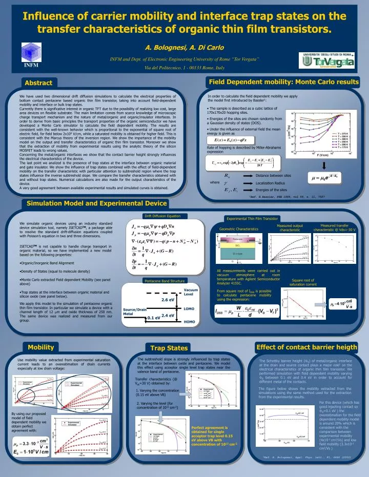
Distance between sites. where. Localization Radius. Energies of the sites. Drift Diffusion Equation. Influence of carrier mobility and interface trap states on the transfer characteristics of organic thin film transistors. A. Bolognesi, A. Di Carlo.

E N D
Distance between sites where Localization Radius Energies of the sites Drift Diffusion Equation Influence of carrier mobility and interface trap states on the transfer characteristics of organic thin film transistors. A. Bolognesi, A. Di Carlo INFM and Dept. of Electronic Engineering University of Rome “Tor Vergata” Via del Politecnico, 1 - 00133 Rome, Italy INFM Field Dependent mobility: Monte Carlo results Abstract In order to calculate the field dependent mobility we apply the model first introduced by Bassler1: We have used two dimensional drift diffusion simulations to calculate the electrical properties of bottom contact pentacene based organic thin film transistor, taking into account field-dependent mobility and interface or bulk trap states. Currently there is significative interest in organic TFT due to the possibility of realizing low cost, large area devices on flexible substrate. The main limitation comes from scarce knowledge of microscopic charge transport mechanism and the nature of metal/organic and organic/insulator interfaces. In order to derive from basic principles the transport properties of the organic semiconductor we have developed a Monte Carlo simulator to calculate the field dependent mobility. The results are consistent with the well-known behavior which is proportional to the exponential of square root of electric field, for field below 2x10⁶ V/cm, while a saturated mobility is obtained for higher field. This is consistent with the Marcus theory of the inversion region. We show the importance of the mobility model on the output and transfer characteristics of organic thin film transistor. Moreover we show that the extraction of mobility from experimental results using the analytic theory of the silicon MOSFET leads to wrong values. Concerning the metal/organic interfaces we show that the contact barrier height strongly influences the electrical characteristics of the device. The last point we analized is the presence of trap states at the interface between organic material and gate insulator. We show the influence of trap states combined with the effect of field-dependent mobility on the transfer characteristic with particular attention to subtreshold region where the trap states influence the inverse subtreshold slope. We compare the transfer characteristics obtained with and without trap states. Numerical calculations are also made for the output characteristics of the device. A very good agreement between available experimental results and simulated curves is obtained. • The sample is described as a cubic lattice of 170x170x20 hopping sites. • Energies of the sites are chosen randomly from a Gaussian density of states (DOS). • Under the influence of external field the mean energy is given as Rate of hopping is described by Miller-Abrahams expression 1Ref. H.Bassler, PRB 1999, vol 59, n. 11, 7507 Simulation Model and Experimental Device Experimental Thin Film Transistor We simulate organic devices using an industry standard device simulation tool, namely ISETCADTM, a package able to resolve the standard drift-diffusion equations coupled with Poisson’s equation in two and three dimensions. Measured transfer characteristic @ Vds=-30 V Measured output characteristic Geometric Characteristics • ISETCADTM is not capable to handle charge transport in organic material, so we have implemented a new model based on the following properties: • Organic/Inorganic Band Alignment • Density of States (equal to molecule density) • Monte Carlo extracted Field dependent Mobility (see panel above) • Trap states at the interface between organic material and silicon oxide (see panel below). All measurements were carried out in vacuum atmosphere at room temperature with Agilent Semiconductor Analyzer 4155C. Square root of saturation corrent Pentacene Band Structure Vacuum Level From square root of IDSS is possible to calculate pentacene mobility using the expression: 2.6 eV We apply this model to the simulation of pentacene organic thin film transistor. In particular we simulate a device with a channel length of 12 m and oxide thickness of 250 nm. The same device was realized and measured from our group. LOMO Source/Drain Metal 2.4 eV 0.1 eV HOMO Effect of contact barrier heigth Mobility Trap States The subtreshold slope is strongly influenced by trap states at the interface between oxide and pentacene. We model this effect using acceptor single level trap states near the valence band of pentacene. Use mobility value extracted from experimental saturation current leads to an overestimation of drain currents expecially at low drain voltage: The Schottky barrier height (B) of metal/organic interface at the drain and source contact plays a major role1 on the electrical characteristics of organic thin film transistor. We performed simulation with field dependent mobility varying B between 0.1 eV and 0.4 eV in order to account for different metal of the contacts. Transfer characteristics (@ Vds=30 V) obtained by: The figure below shows the mobility extracted from the simulations using the same method used for the extraction from the experimental results. 1. Varying the concentration (0.15 eV above VB) For this device (which has good injecting contact so B=0.1 eV ) the overestimation for the field dependent mobility model is around 20% which is consistent with the comparison between experimental mobility (4x10⁻³ cm2/Vs) and low field mobility (3.3x10⁻³ cm2/Vs ) 2. Varying the level (for concentration of 1012 cm-2) By using our proposed model of field dependent mobility we obtain perfect agreement with: Perfect agreement is obtained for single acceptor trap level 0.15 eV above VB with concentration of 1012 cm-2 1Ref. A. Bolognesi, Appl. Phys. Lett., 81, 4646 (2002)