Download
1 / 136
1.47k likes | 1.86k Vues
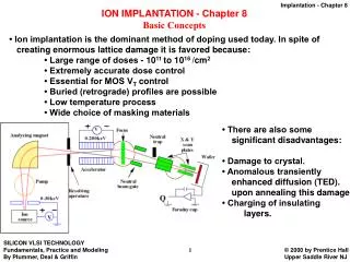
Chapter 8 Ion Implantation. Hong Xiao, Ph. D. hxiao89@hotmail.com www2.austin.cc.tx.us/HongXiao/Book.htm. Objectives. List at least three commonly used dopants Identify three doped areas Describe the advantages of ion implantation Describe major components of an implanter

E N D
Chapter 8Ion Implantation Hong Xiao, Ph. D. hxiao89@hotmail.com www2.austin.cc.tx.us/HongXiao/Book.htm www2.austin.cc.tx.us/HongXiao/Book.htm
Objectives • List at least three commonly used dopants • Identify three doped areas • Describe the advantages of ion implantation • Describe major components of an implanter • Explain the channeling effect • Relationship of ion range and ion energy • Explain the post-implantation annealing • Identify safety hazards www2.austin.cc.tx.us/HongXiao/Book.htm
Ion Implantation • Introduction • Safety • Hardware • Processes • Summary www2.austin.cc.tx.us/HongXiao/Book.htm
Materials Etch PR strip Test Metalization Wafers Photo-lithography Thermal Processes Dielectric deposition Packaging Masks Implant PR strip CMP Final Test Design Wafer Process Flow IC Fab www2.austin.cc.tx.us/HongXiao/Book.htm
Introduction: Dope Semiconductor • What is Semiconductor? • Why semiconductor need to be doped? • What is n-type dopant? • What is p-type dopant? www2.austin.cc.tx.us/HongXiao/Book.htm
Introduction • Dope semiconductor • Two way to dope • Diffusion • Ion implantation • Other application of ion implantation www2.austin.cc.tx.us/HongXiao/Book.htm
Dope Semiconductor: Diffusion • Isotropic process • Can’t independently control dopant profile and dopant concentration • Replaced by ion implantation after its introduction in mid-1970s. www2.austin.cc.tx.us/HongXiao/Book.htm
Dope Semiconductor: Diffusion • First used to dope semiconductor • Performed in high temperature furnace • Using silicon dioxide mask • Still used for dopant drive-in • R&D on ultra shallow junction formation. www2.austin.cc.tx.us/HongXiao/Book.htm
Dopant Oxide Deposition Deposited Dopant Oxide SiO2 Si Substrate www2.austin.cc.tx.us/HongXiao/Book.htm
Oxidation SiO2 Si Substrate www2.austin.cc.tx.us/HongXiao/Book.htm
Drive-in SiO2 Doped junction Si Substrate www2.austin.cc.tx.us/HongXiao/Book.htm
Strip and Clean SiO2 Doped junction Si Substrate www2.austin.cc.tx.us/HongXiao/Book.htm
Dope Semiconductor: Ion Implantation • Used for atomic and nuclear research • Early idea introduced in 1950’s • Introduced to semiconductor manufacturing in mid-1970s. www2.austin.cc.tx.us/HongXiao/Book.htm
Dope Semiconductor: Ion Implantation • Independently control dopant profile (ion energy) and dopant concentration (ion current times implantation time) • Anisotropic dopant profile • Easy to achieve high concentration dope of heavy dopant atom such as phosphorus and arsenic. www2.austin.cc.tx.us/HongXiao/Book.htm
Misalignment of the Gate Gate Oxide Metal Gate Metal Gate p+ S/D p+ S/D n-Si n-Si Aligned Misaligned www2.austin.cc.tx.us/HongXiao/Book.htm
Ion Implantation, Phosphorus P+ SiO2 Poly Si n+ n+ P-type Silicon www2.austin.cc.tx.us/HongXiao/Book.htm
Comparison of Implantation and Diffusion Doped region SiO2 PR Si Si Junction depth Ion implantation Diffusion www2.austin.cc.tx.us/HongXiao/Book.htm
Comparison of Implantation and Diffusion www2.austin.cc.tx.us/HongXiao/Book.htm
Ion Implantation Control • Beam current and implantation time control dopant concentration • Ion energycontrols junction depth • Dopant profile is anisotropic www2.austin.cc.tx.us/HongXiao/Book.htm
Applications of Ion Implantation www2.austin.cc.tx.us/HongXiao/Book.htm
Other Applications • Oxygen implantation for silicon-on-insulator (SOI) device • Pre-amorphous silicon implantation on titanium film for better annealing • Pre-amorphous germanium implantation on silicon substrate for profile control • …... www2.austin.cc.tx.us/HongXiao/Book.htm
Some Fact about Phosphorus www2.austin.cc.tx.us/HongXiao/Book.htm
Some Fact about Arsenic www2.austin.cc.tx.us/HongXiao/Book.htm
Some Fact about Boron www2.austin.cc.tx.us/HongXiao/Book.htm
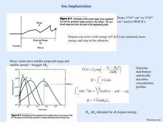
Stopping Mechanism • Ions penetrate into substrate • Collide with lattice atoms • Gradually lose their energy and stop • Two stop mechanisms www2.austin.cc.tx.us/HongXiao/Book.htm
Two Stopping Mechanism • Nuclear stopping • Collision with nuclei of the lattice atoms • Scattered significantly • Causes crystal structure damage. • electronic stopping • Collision with electrons of the lattice atoms • Incident ion path is almost unchanged • Energy transfer is very small • Crystal structure damage is negligible www2.austin.cc.tx.us/HongXiao/Book.htm
Stopping Mechanism • The total stopping power Stotal = Sn + Se • Sn: nuclear stopping, Se: electronic stopping • Low E, high A ion implantation: mainly nuclear stopping • High E, low A ion implantation, electronic stopping mechanism is more important www2.austin.cc.tx.us/HongXiao/Book.htm
Stopping Mechanisms Ion Random Collisions (S=Sn+Se) Channeling (SSe) Back Scattering (SSn) www2.austin.cc.tx.us/HongXiao/Book.htm
Stopping Power and Ion Velocity I II III Nuclear Stopping Stopping Power Electronic Stopping Ion Velocity www2.austin.cc.tx.us/HongXiao/Book.htm
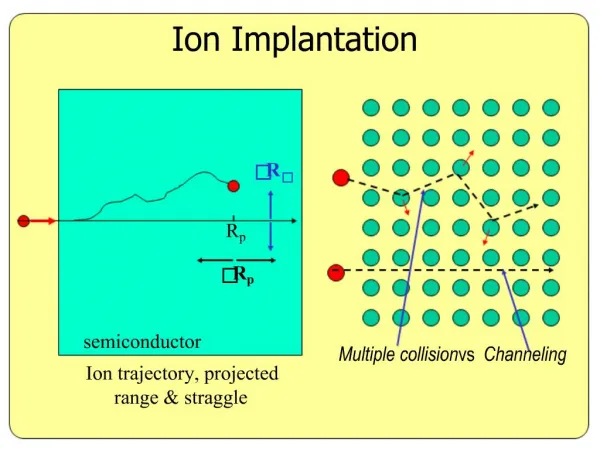
Ion Trajectory and Projected Range Vacuum Substrate Collision Ion Trajectory Ion Beam Projected Range Distance to the Surface www2.austin.cc.tx.us/HongXiao/Book.htm
Ion Projection Range ln (Concentration) Projected Range Substrate Surface Depth from the Surface www2.austin.cc.tx.us/HongXiao/Book.htm
Projected Range in Silicon 1.000 P B Projected Range (mm) 0.100 As Sb 0.010 10 100 1000 Implantation Energy (keV) www2.austin.cc.tx.us/HongXiao/Book.htm
Barrier Thickness to Block 200 keV Ion Beam 1.20 1.00 B 0.80 0.60 P Mask Thickness (micron) 0.40 As 0.20 Sb 0.00 PR Si SiO2 Si3N4 Al www2.austin.cc.tx.us/HongXiao/Book.htm
Implantation Processes: Channeling • If the incident angle is right, ion can travel long distance without collision with lattice atoms • It causes uncontrollable dopant profile Lots of collisions Very few collisions www2.austin.cc.tx.us/HongXiao/Book.htm
Channeling Effect Lattice Atoms Channeling Ion Collisional Ion q Wafer Surface www2.austin.cc.tx.us/HongXiao/Book.htm
Post-collision Channeling Collisional Channeling Collisional q Wafer Surface www2.austin.cc.tx.us/HongXiao/Book.htm
Post-collision Channeling Collisional Channeling Collisional Dopant Concentration Distance from surface www2.austin.cc.tx.us/HongXiao/Book.htm
Implantation Processes: Channeling • Ways to avoid channeling effect • Tilt wafer, 7° is most commonly used • Screen oxide • Pre-amorphous implantation, Germanium • Shadowing effect • Ion blocked by structures • Rotate wafer and post-implantation diffusion www2.austin.cc.tx.us/HongXiao/Book.htm
Shadowing Effect Ion Beam Polysilicon Doped Region Substrate Shadowed Region www2.austin.cc.tx.us/HongXiao/Book.htm
Shadowing Effect After Annealing and Diffusion Polysilicon Doped Region Substrate www2.austin.cc.tx.us/HongXiao/Book.htm
Q & A • Why don’t people use channeling effect to create deep junction without high ion energy? • Ion beam is not perfectly parallel. Many ions will start to have a lot of nuclear collisions with lattice atoms after they penetrating into the substrate. Some ions can channel deep into the substrate, while many others are stopped as the normal Gaussian distribution. www2.austin.cc.tx.us/HongXiao/Book.htm
Damage Process • Implanted ions transfer energy to lattice atoms • Atoms to break free • Freed atoms collide with other lattice atoms • Free more lattice atoms • Damage continues until all freed atoms stop • One energetic ion can cause thousands of displacements of lattice atoms www2.austin.cc.tx.us/HongXiao/Book.htm
Lattice Damage With One Ion Light Ion Damaged Region Heavy Ion Single Crystal Silicon www2.austin.cc.tx.us/HongXiao/Book.htm
Implantation Processes: Damage • Ion collides with lattice atoms and knock them out of lattice grid • Implant area on substrate becomes amorphous structure Before Implantation After Implantation www2.austin.cc.tx.us/HongXiao/Book.htm
Implantation Processes: Anneal • Dopant atom must in single crystal structure and bond with four silicon atoms to be activated as donor (N-type) or acceptor (P-type) • Thermal energy from high temperature helps amorphous atoms to recover single crystal structure. www2.austin.cc.tx.us/HongXiao/Book.htm
Thermal Annealing Lattice Atoms Dopant Atom www2.austin.cc.tx.us/HongXiao/Book.htm
Thermal Annealing Lattice Atoms Dopant Atom www2.austin.cc.tx.us/HongXiao/Book.htm
Thermal Annealing Lattice Atoms Dopant Atom www2.austin.cc.tx.us/HongXiao/Book.htm
Thermal Annealing Lattice Atoms Dopant Atom www2.austin.cc.tx.us/HongXiao/Book.htm
Thermal Annealing Lattice Atoms Dopant Atom www2.austin.cc.tx.us/HongXiao/Book.htm