Download
1 / 37
370 likes | 539 Vues
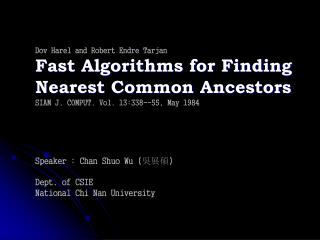
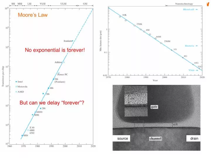
Moore’s Law. No exponential is forever!. But can we delay “forever”?. source. drain. Cavin, Hutchby, Zhirnov, Bourianoff. Cavin, Hutchby, Zhirnov, Bourianoff. Graphene M onolayer. Phonon Frequency (cm -1 ). M. Γ. K. Γ.

E N D
Moore’s Law No exponential is forever! But can we delay “forever”? source drain
Graphene Monolayer Phonon Frequency (cm-1) M Γ K Γ Future of Microelectronics: The beginning of the end or the end of the beginning?Sanjay Banerjee, Univ. of Texas Task 2:Spintronics in DMS Task 1: Logic Devices with Alternate State Variables Pseudospintronics on Graphene: UT, UTD, Maryland MQCA:ND DMS: A&M, Maryland, UT Phasetronics: UT Path Integral Monte Carlo: ASU, UT Task 5: Nanoscale Characterization UTD Task 3: Nanoscale Thermal Management UIUC, NCSU Task 4: Nano plasmonic interconnects Rice
South West Academy of Nanoelectronics TI, Intel, IBM, Micron, AMD, Freescale, NIST Texas ETF
The Scale of Things – Nanometers and More Ant ~ 5 mm Dust mite 200 mm Fly ash ~ 10-20 mm Things Natural Things Manmade 1 cm 10 mm 10-2 m Head of a pin 1-2 mm The Challenge 1,000,000 nanometers = 10-3 m 1 millimeter (mm) MicroElectroMechanical (MEMS) devices 10 -100 mm wide Microwave 0.1 mm 100 mm 10-4 m Human hair ~ 60-120 mm wide 0.01 mm 10 mm Microworld 10-5 m Pollen grain Red blood cells Infrared Red blood cells with white cell ~ 2-5 mm Zone plate x-ray “lens”Outer ring spacing ~35 nm 1,000 nanometers = 10-6 m 1 micrometer (mm) Visible Smaller is different! Fabricate and combine nanoscale building blocks to make useful devices, e.g., a photosynthetic reaction center with integral semiconductor storage. 0.1 mm 100 nm 10-7 m Ultraviolet Self-assembled, Nature-inspired structureMany 10s of nm 0.01 mm 10 nm Nanoworld 10-8 m ~10 nm diameter Nanotube electrode ATP synthase 10-9 m 1 nanometer (nm) Carbon buckyball ~1 nm diameter More is different! Soft x-ray Carbon nanotube ~1.3 nm diameter DNA ~2-1/2 nm diameter 10-10 m 0.1 nm Quantum corral of 48 iron atoms on copper surface positioned one at a time with an STM tip Corral diameter 14 nm Atoms of silicon spacing ~tenths of nm Office of Basic Energy Sciences Office of Science, U.S. DOE Version 10-07-03, pmd
Subthreshold leakage is diffusion current from S to D (as in BJT) S= ln10 kT/q (1 + Cd/Cox) SWAN
Effective Bandstructure effective mass, m*, is inversely related to curvature of bands, and depends on crystal orientation and strain. Density of states m* is related to geometric mean of bandstructure m*. Conductivity m* is harmonic mean of bandstructure m*.
Gapless, unless GNR Electric field induced gap in bi-layer Linear E(k) at K point; Dirac massless fermions Min, Sahu, Banerjee, MacDonald, PRB (2007) GrapheneBandstructure Uext=0 , Egap=0 k space
dIT/dV 0 0 V Pseudospintronics in Bilayers at low T, high B • Charge-neutral superfluid: Bose-Einstein condensate of excitons! • Electron-hole pairing enhanced interlayer conductance with NDR I. Spielman et al., Phys. Rev. Lett. 84, 5808 (2000)
eB c = me Electrons in a Magnetic Field: Landau Levels Atomic Levels: Electrons in Atomic Orbitals: E3 B ħc Electrons in Magnetic Field: E2 ħc E1 ħc E0 • En = (n + 1/2) hc (Landau levels) • Macroscopic degeneracy: eB/h = 2.42´1010cm-2 T
hc B Quantum Hall Effect B B Vxy I Resistance Filling factor n = 2 n = 1 (von Klitzing, 1980) Magnetic Field
Spin Precession Precession Starts on application of Magnetic FieldB H = - μ. B = MAGNETIC FIELD μ X H Polar angles (θ, φ) SPIN mħ Electron Spin MAGNETIC MOMENT electron precession in magnetic field
cos(/2) +sin(/2) eiφ cos(/2) +sin(/2) eiφ A B top layer: bottom layer: cos(/2) +sin(/2) eiφ Quantum 2-Level Systems
nT = 1/2 d ~ lB nB = 1/2 Pseudo-spintronic devices • Device consisting of two electron and/or hole layers in close proximity • Inter-layer electron-electron interaction strong “layer” (pseudo-spin) degree of freedom uncertain • Charge transport intimately determined by the dynamics of the pseudo-spin degree of freedom zi zj wi wj
Intra-layer vs Inter-layer interaction B e2 Einter= e d e2 Eintra= e lB d Eintra d = Einter lB • Expect exciting physics when d/lb 1
I + - Vxy I Vxx Quantum Hall Effect-Counterflow transport in GaAs-AlGaAs • Vanishing counterflow longitudinal and Hall resistivities at n=1 QHS • Charge-neutral superfluid: Bose-Einstein condensate of excitons! • Electron-hole pairing enhanced interlayer conductance E. Tutuc et al., Phys. Rev. Lett. 93, 036802 (2004).
Graphene bilayer with excitons formed by MOS gate Prediction of above room temperature existence of electron-hole condensate holes in valence band electrons in conduction band + • Room-Temperature Superfluidity in Graphene Bilayers?, • Min, Bistritzer, Su, MacDonald • How to make a bilayer exciton condensate flow, • Su, MacDonald
Bi-layer pseudoSpin Field Effect Transistor (BiSFET)Banerjee, Register, Tutuc and Macdonald “Bilayer pseudoSpin Field Effect Transistor (BiSFET): a proposed new logic device” S.K. Banerjee, L.F. Register, E.Tutuc, D.Reddy and A. Macdonald., IEEE EDL, accepted (2008); also patent disclosure
BisFET simulated output characteristics as a function of interlayer bias and gate bias. VG’ puts the device in an unbalanced state, leading to lower currents Layer2:Holes [p] Layer1:Electrons [n] Tc = 0.1Ef/kB; Tc = 300K implies n=p=4.9x1012 cm-2 which is possible by gating Bose condensation of excitons [e-h pairs] Inter layer bias Many body tunneling Inter layer current
Inverter layout with complementary BisFETs and SPICE simulation 1.0 nm EOT, gate L=10 nm, corresponding to the Josephson length, and W=20 nm. Clock frequency= 100 GHz and Vclock,peak25 mV with 2.5 ps rise time. Input and output signals were subject to a fan-in and fan-out of 4 inverters. Current MOSFETs consume ~100 aJ per switching and 2020 “end of the roadmap CMOS will consume ~5 aJ [www.itrs.net]. Energy consumed per switching operation per BiSFET= 0.008 aJ! (2X Landauer limit)
OR and NAND Gate • Clock: • Vlow = 0mV ; Vhigh= 25mV • Rise time= 2.5 ps • Fall time = 2.5 ps • Pulse width = 2.5ps • Pulse period =10 ps • Frequency of cock = 100 GHz • Delay between clock and input signal is 2.5 ps • Maximum number of inverters the OR gate can drive: 6 • Energy per operation: • For OR GATE (load = 4 inverters) total energy for 4 operations: 133.7 x 1E-21 J • Average Energy per operation 33.4 x 1E-21 J • For NAND GATE(load = 4 inverters) total energy for 4 operations: 121.81x1E-21 J • Average Energy per operation 30.45 x 1E-21 J
The Collective FET vision kBT/nq ~ about 25mV/n
Graphene MOSFET Fabrication and Modeling Quantum Capacitance in Graphene VTG and carrier density, n, relation Carrier density in the channel induced by VTG
R vs (VTG-VDirac) with model: 15nm Al2O3 Top-gated FET • Thinner dielectric layer • lower remote charge impurities in oxide • Lower initial carriers • less carrier scattering • Higher mobility • Mobility independent of T God made solids; surfaces on the other hand are the work of the devil. (Pauli)
All Graphene Electronics DARPA Carbon Era Rf Applications (CERA) program with IBM LNA, interconnects, …
Nearest neighbor (NN) tight binding Hamiltonian: , for NN, 0 otherwise. self-consistent potential. Tight Binding Model of Graphene Perfect armchair graphene ribbon showing equal no. of atoms in successive slices. Corresponding band structures: No. of atoms in the slice = 7, 8 and 9
T(E) vs. E for a 7.63 nm wide graphene channel having different roughness. r = 0.5 » random, r = 1 » perfect. T(E) vs. E [different roughness (identical Wch)]
Phasetronics: AB device with Rashba Effect Register, Banerjee EX OR Gate A=0, B=0 C=0 A=0, B=1 C=1 A=1, B=0 C=1 A=1, B=1 C=0 A=0 Precession of phase + C B=0 State 0: Electron transmission is suppressed State 1: Electron transmission is permitted
Resonant Injection Enhanced Field-Effect Transistor Patent disclosure, Register, Banerjee
ON/OFF states of RIEFET • ON state (Vg=150mV in following examples): • The multiple quantum-wells below the gate serve as a nearly transparent high-order band pass filter for electrons; • OFF state (Vg=0mV): • The gate not only raises the channel potential directly beneath the gate relative to the source, but destroys the inter-well resonances and reduce access to the channel even for electrons with sufficient thermal energy. Energy levels of quantum states Top gate Aligned Transport direction Energy levels of quantum states Top gate Misaligned Transport direction
Spintronics- Datta-Das Transistor Electrons quantum mechanically can be viewed as a spinning top which can point “up” or “down”!
A M B C A 0 0 -1 0 1 1 1 1 B Out C Nanomagnet-Based Logic- MQCAWolfgang Porod and Gary Bernstein, Univ. Notre Dame Binary wire Majority gate Inverter Programmable 2-input AND or OR gate.
What is needed in the new switch? CMOS ca 2020 • Energy ~ 10 aJ/op; power~ 107 W/cm2 • Speed ~ 0.1 ps/op (10 THz fT; 100 GHz circuit) • Size ~ Lg 5 nm; cell ~ 100 nm, IDN~ 3 mA/µm • Density ~ 1010 cm-2; BIT ~100 GBit/ns/cm2 • Cost ~ 10-12 $/gate Speed = CV/I Active Power = CV2f Stand-by Power = Sub-VT, gate leakage • Desirable Attributes • Energy efficiency • Speed (performance, noise) • Room T operation (non-equilibrium devices?) • Size (device/ wafer): capacitance, fan-out • Gain; uni-directional signal flow (I/O isolation) • Reliability, manufacturability, cost • CMOS compatibility (process, topology) 0.01 aJ/op 100GHz Yes 10 nm, FO=4 Yes ??? ??? Not Yet! Mission Accomplished