Download
1 / 38
380 likes | 508 Vues
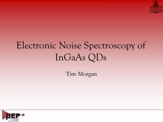
Electronic Noise Spectroscopy of InGaAs QDs. Tim Morgan. Outline. Motivation Theory of Electrical Transport and Noise Experimental Techniques Discussion & Results Conclusions. What is a Quantum Dot?. Single Atom. Many Atoms. A Few Atoms Confined.

E N D
Electronic Noise Spectroscopy of InGaAs QDs Tim Morgan
Outline • Motivation • Theory of Electrical Transport and Noise • Experimental Techniques • Discussion & Results • Conclusions Noise in QDs 7.23.08
What is a Quantum Dot? Single Atom Many Atoms A Few Atoms Confined • Single atom: Discrete energy level transitions • Many atoms: continum of energy levels • A Few Atoms Confined: lower energy levels discrete because of confinement ~30 nm Noise in QDs 7.23.08
Quantum Dot Devices QD Laser byz.org Quantum Dots cqd.eecs.northwestern.edu Single Photon Emitter Infrared Detectors Igor L. Medintz, et. al. Nature Materials 2003 Biosensors Noise in QDs 7.23.08
The Nature of Noise in QDs • What is the source of noise in QDs? • Does noise in QDs differ from bulk? • Is there a correlation of noise, defects and QDs? Noise in QDs 7.23.08
The Plan UNDERSTANDING Noise Measurements Noise Spectroscopy Mobility & Carrier Concentration Hall PL Electronic structure Morphology AFM In0.35Ga0.65As QDs MBE Noise in QDs 7.23.08
QD Formation InGaAs fluxes When critical thickness is reached, the strain is relaxed and thus 3D islands (quantum dots) are formed. - I’m now happy!! Strain has built up! - I’m very uncomfortable!! 2D InGaAswetting layer GaAs substrate Used with permission of Jihoon Lee Noise in QDs 7.23.08
Atomic Force Microscopy Surface data • Height • Diameter • Density Noise in QDs 7.23.08
Photoluminescence Noise in QDs 7.23.08
Hall Effect • Transport Info • Mobility • Carrier • Concentration • Hall Coefficient • Conductivity • Primary Carrier Noise in QDs 7.23.08
Noise Spectroscopy • Measure voltage perpendicular to bias direction • The fluctuations in voltage are measured over a time period • SV is the average change in voltage in frequency of 1 Hz Noise in QDs 7.23.08
Thermal Noise • Frequency Independent • Dominant at high frequencies • Due to random fluctuations from Brownian motion of electrons Noise in QDs 7.23.08
Flicker noise • Dominant at lower frequencies • Due to conductivity fluctuations • Can arise from both carrier and mobility fluctuations Noise in QDs 7.23.08
Why 1/f Dependence? Tail States (Defects) Noise in QDs 7.23.08
Generation-Recombination Noise • Lorentzian with characteristic frequency • Apperas as a shoulder in the noise spectrum • Due to electrons being emitted and recombining from deep traps Noise in QDs 7.23.08
Total Noise Measured Spectra Noise in QDs 7.23.08
Sample Creation • MBE Growth • Solid Source Riber 32 P • RHEED monitoring • Post Growth • AFM • PL • Cryostat @ 10 K • YAG laser 20 W/cm2, 532 nm • ~ 20 μm spot size Noise in QDs 7.23.08
The Structure Sample # MLs 1500 Å GaAs: Si T=1133ºC S1 0 200 Å GaAs: undoped S2 6 S3 9 InGaAs QD layer S4 11 200 Å GaAs: undoped S5 13 5000 Å GaAs: Si T=1133ºC 5000 Å GaAs buffer GaAs (001) SI Noise in QDs 7.23.08
Morphology • No QDs with 0 or 6 ML samples 9 ML Height: 33 ± 0.5 Å Density: 3.8 × 1010cm-2 11 ML Height: 47 ± 0.3 Å Density: 8.4 × 1010cm-2 13 ML Height: 53 ± 0.4 Å Density: 7.2 × 1010cm-2 Noise in QDs 7.23.08
PL • Red shift in energy • Single size distribution • Decrease in integral intensity • All results correlate well with AFM data • Increase in height • Same FWHM trend Noise in QDs 7.23.08
Sample Preparation 270 nm Au 20 nm Ni 75 nm AuGe 30 µm Greek Cross • Wet Etch • Metallization Noise in QDs 7.23.08
Contact Optimization lT c c AuGe/Ni/Au d rs Rs Rs dx Dopant 0 -l x • Annealing: minimize barrier to create Ohmic contacts • IV Testing: Verify Ohmiccontacs made • TLM Measurements: determince contact resistance Noise in QDs 7.23.08
Finished Structures 13 ML All samples meet Noise in QDs 7.23.08
Hall Measurements • Hall Measurements • Mobility • Carrier concentration • Resistance measurements Noise in QDs 7.23.08
Mobility Noise in QDs 7.23.08
Carrier Concentration Noise in QDs 7.23.08
DLNS: Setup & Experiments • Setup • Shielded sample • Power supply: battery pack and series of resistors • Low noise preamplifier with band filter • Noise spectrum analyzer • Experiments • Temperature dependence: 82 K – 390 K, fixed bias • Room temperature: several biases • Low temperature (82 K): several biases Noise in QDs 7.23.08
Noise Curves 0 ML 300 K • Series of spectra at fixed temperatures and various biases • Fit each specturm with all components of noise • Extract fit parameters for component breakdown analysis Noise in QDs 7.23.08
Flicker Noise • Fit Parameter: • Determine the Hooge Parameter at 300 K and 82 K 0 ML Sample at 300 K Noise in QDs 7.23.08
Hooge Comparison 300 K 82 K Noise in QDs 7.23.08
QD Height Comparison 300 K 82 K Noise in QDs 7.23.08
QD Density Comparison 300 K 82 K Noise in QDs 7.23.08
Two Views Shoulders Peaks Noise in QDs 7.23.08
GR Analysis • A different expression: • Peaks reveal the activation and ionization energy • lnSmaxvslnω ionization energy • 1/kBTmaxvslnω activation energy • Capture cross section: • Trap density: Noise in QDs 7.23.08
Analysis Plots 11 ML 11 ML Ionization Energy Activation Energy Noise in QDs 7.23.08
GR Summary Noise in QDs 7.23.08
Conclusions • Sources of Noise in QDs • GR Traps with activation energies of 0.74, 0.49, 0.34, 0.18 and 0.1 eV • Tail states from crystal imperfections • Noise in QDs does differ from bulk • Flicker noise decreases with the insertion of In0.35Ga0.65As and the formation of QDs • Flicker noise decreases with increase of height and density • Additional GR Trap in QD samples not present in bulk • Correlation of noise, defects and QDs • GR traps give rise to GR Noise • QDs lowers flicker noise Noise in QDs 7.23.08
Future Work • Study Gated QD samples • Change where current flows to determine which layer noise arises from • Study QDs with vertical biasing • Vary doping to change Fermi level • Enhance noise when in resonance with traps • Inject minority carriers with light into QD samples • Determine energy positions relative to conduction band • QDIPs • Look at noise in a QD device and show its detection limit because of the noise Noise in QDs 7.23.08