Download
1 / 34
350 likes | 357 Vues
Layout techniques for increased radiation tolerance in commercial CMOS for pixel readout circuits. W. Snoeys Microelectronics Group, EP Division, CERN Representing the ALICE pixel, LHCB RICH and RD49 collaborations CERN EP Seminar October 19, 1998. Michael Campbell Eugenio Cantatore

E N D
Layout techniques for increased radiation tolerance in commercial CMOS for pixel readout circuits W. Snoeys Microelectronics Group, EP Division, CERN Representing the ALICE pixel, LHCB RICH and RD49 collaborations CERN EP Seminar October 19, 1998 Walter SNOEYS - CERN - EP - MIC
Michael Campbell Eugenio Cantatore Ken Wyllie Domenico Minervini Roberto Dinapoli Elena Pernigotti Katelijn Vleugels Pierre-Marie Signe Federico Faccio Etam Noah Giovanni Anelli Marco Delmastro I. Ropotar L. Casagrande Bettina Mikulec Milo Luptak Peter Sonderegger Carlos Lourenco Other contributors and Acknowledgements • Erik Heijne • Pierre Jarron • Alessandro Marchioro • Mike Letheren • Willy Sansen • Franco Corsi • Michael Burns • Michel Morel • Paolo Martinengo • Stefania Saladino • Fabio Formenti • Franco Meddi et al. • Wolfgang Klempt • Federico Antinori Walter SNOEYS - CERN - EP - MIC
OVERVIEW • Problem with total dose in standard CMOS technologies • Principle and effectiveness of layout techniques • Design description and electrical results on pixel prototypes • Irradiation results on pixel prototype • Design implications • Conclusions and perspectives Walter SNOEYS - CERN - EP - MIC
Total ionizing irradiation dose problem in commercial CMOS • Radiation induces positive fixed oxide charge and interface states • Vt - shift • weak inversion slope change • mobility change • LEAKAGE in NMOS transistors Example from 0.5 mm technology (tox ~ 10 nm) Walter SNOEYS - CERN - EP - MIC
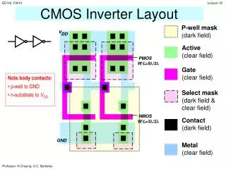
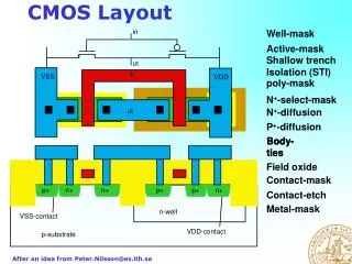
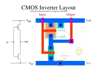
NMOS TRANSISTOR LEAKAGE ENCLOSED TRANSISTOR LAYOUT Example from 0.5 mm technology (tox ~ 10 nm) Walter SNOEYS - CERN - EP - MIC
NMOS INTER-TRANSISTOR LEAKAGE GUARD RINGS Drain1 Well/ Substrate Source1 Gate1 P+ Source2 Gate2 N+ Walter SNOEYS - CERN - EP - MIC
A B C D Transistor Threshold shift • Tunneling of trapped charge in thin oxides • DVT ~ 1/tox2 for tox > 10nm • DVT ~ 1/tox3 for tox < 10 nm After N.S. Saks, M.G. Ancona, and J.A. Modolo, IEEE Trans.Nucl.Sci., Vol. NS-31 (1984) 1249 Walter SNOEYS - CERN - EP - MIC
Layout Techniques for Radiation Tolerance : Conclusion • N-channel transistor leakage solved by enclosed geometry layout • N-channel inter-transistor (field) leakage solved by guard rings • Radiation induced trapped charge and interface : - reduced for thin oxides - for very thin oxides (tox < 10 nm) reduced much more • => radiation induced transistor parameter shifts smaller and smaller in deeper submicron technologies Walter SNOEYS - CERN - EP - MIC
A Pixel Readout Prototype in Radiation Tolerant Layout shaper Rfb comparator Cfb data FF delay logic preamp strobe & polarity Clk threshold setting Cin test FF mask FF leakage current compensation analog test input Leakage current compensation after F. Krummenacher, Nucl. Instr. and Meth., Vol. A305 (1991) 527-532, modified to accommodate both positive and negative detector leakage current Walter SNOEYS - CERN - EP - MIC
ALICE1 ELECTRICAL RESULTS Detector leakage current compensation • No pixel threshold change • Noise increases with detector leakage current as expected Walter SNOEYS - CERN - EP - MIC
LHC2TEST/ALICE1TEST ELECTRICAL RESULTS Timewalk Walter SNOEYS - CERN - EP - MIC
ELECTRICAL RESULTS Timewalk on LHC1 for comparison Walter SNOEYS - CERN - EP - MIC
A Pixel Readout Prototype in Radiation Tolerant Layout :Summary Electrical Results • for a detector leakage current increase of 1 to 200nA : - threshold variation ~ 1% - noise increase from about 200e RMS to 400e RMS for holes, and to 350e RMS for electrons. • threshold variable between 2000 to 15000 holes or electrons • threshold spread too large (400 - 500 e RMS) • timewalk within 25 ns for only a few 100 electrons above threshold Walter SNOEYS - CERN - EP - MIC
ALICE2TEST ELECTRICAL RESULTS Threshold uniformity and noise • Threshold variation about 160 e rms, without 3 bit threshold adjust • Noise about 220 e rms • 1 mV ~ 100 e Walter SNOEYS - CERN - EP - MIC
ALICE2TEST ELECTRICAL RESULTS Average Threshold, Threshold variation and average noise Walter SNOEYS - CERN - EP - MIC
ALICE2TEST (0.25 mm) :Summary Electrical Results • Characterization in progress • Already established : - minimum threshold 1500 e or below - 3 bit threshold adjust works - detector leakage current compensation works up to several 100 nA/pixel - both dynamic and static counter based delay lines work Walter SNOEYS - CERN - EP - MIC
LHC2TEST/ALICE1TESTEvolution of Threshold and Threshold Variation with Xray Dose Walter SNOEYS - CERN - EP - MIC
LHC2TEST/ALICE1TESTEvolution of Power Consumption with Xray Dose • Analog no change • Digital can be explained by Vt shift • Validates layout approach on global scale Walter SNOEYS - CERN - EP - MIC
LHC2TEST/ALICE1TESTIonizing Particle Irradiation in NA50 • Severe degradation only after 1.7 Mrad in two days • After 42 hours beam was off for a couple of hours, some recovery visible • Drop in lower plot below 130 before 50 hours is artifact, all pixels responded • Irradation continued to about 3 Mrad after none of the pixels responded any more Walter SNOEYS - CERN - EP - MIC
Ionizing Particle Irradiation in NA50 : anneal • Some pixels start to respond after 1 week of annealing at room temperature • The last week of anneal was carried out at 100 C => slope change Walter SNOEYS - CERN - EP - MIC
Irradiation Degradation MechanismMeasured NMOS transistor VT shift Walter SNOEYS - CERN - EP - MIC
Irradiation Degradation Mechanism • Introduced measured Vt - shift data to simulate degradation • Vt - shift causes preamplifier feedback to push shaper input transistor out of saturation • Confirmed by correlation of operating margin and irradiation dose Walter SNOEYS - CERN - EP - MIC
LHC2TEST/ALICE1TESTRadiation Tolerance : Summary • Irradiation tests done with 10 keV X-rays, Gamma 60Co, 6.5 MeV protons, and electrons in NA50 • No large increase in supply currents with dose => rad tolerant layout techniques prevent leakage • Serious degradation (= severe pixel threshold increase) sets in only after ~600 krads with Xrays and ~1 Mrad or higher for the other sources (e.g. 1.7 Mrad for NA 50 beam) Walter SNOEYS - CERN - EP - MIC
LHC2TEST/ALICE1TESTRadiation Tolerance :Summary • Degradation mechanism explained through Vt shift • Significant recovery (annealing) after a relatively short time Walter SNOEYS - CERN - EP - MIC
ALICE2TEST ChipEvolution of power supply currents with X-ray dose (10 keV X-rays at 4 krad/min) Walter SNOEYS - CERN - EP - MIC
ALICE2TEST ChipEvolution of average threshold, threshold dispersion and noise with X-ray dose Walter SNOEYS - CERN - EP - MIC
ALICE2TEST Radiation Tolerance : Summary • Irradiation tests done with 10 keV X-rays @ 4 krad/min • No large increase in supply currents with dose => rad tolerant layout techniques prevent leakage • Functionality preserved up to 30 Mrad, parametric degradation (noise and threshold dispersion increase) acceptable, also after anneal • Also confirmed in proton beam up to 1.5e15 protons/cm2 Walter SNOEYS - CERN - EP - MIC
Layout for Radiation Tolerance : Design Implications Modeling of Transistors in Enclosed Geometry Walter SNOEYS - CERN - EP - MIC
Layout for Radiation Tolerance : Design Implications Modeling of Transistors in Enclosed Geometry • I - V characteristics (SPICE models) Note : to obtain W/Leff = .1 …. IMPOSSIBLE ! => accurate NMOS current mirrors difficult • Matching : non-uniform current flow ! • Noise • Before and after irradiation ! Walter SNOEYS - CERN - EP - MIC
Layout for Radiation Tolerance : Design Implications Circuit Density : • Digital : there clearly is a penalty for the same technology. However, one should compare not to the same technology but to a radiation hard/tolerant alternative. • Analog : example showed certain circuit topologies (making use of accurate NMOS mirrors for instance…) should be avoided. In that case small penalty even for same technology. • Number of metal layers plays a big role Walter SNOEYS - CERN - EP - MIC
Layout for Radiation Tolerance : Design Implications CAD Environment (!!!) • Digital library = full custom • Verification routines : DRC, extraction, LVS ALL require some modification Walter SNOEYS - CERN - EP - MIC
CONCLUSIONS AND PERSPECTIVES • Special layout + thin gate oxide = radiation tolerance • Special layout techniques have made a pixel readout prototype implemented in a - commercial 0.5 mm CMOS technology radiation tolerant up to ~ 1 Mrad. - commercial 0.25 mm CMOS technology radiation tolerant up to 30 Mrad. • Density, power-speed performance, and radiation tolerance => deeper submicron • Design implications • Note : Single event effects Walter SNOEYS - CERN - EP - MIC
CONCLUSIONS AND PERSPECTIVES • Thinner gate oxide helps to reduce radiation induced transistor parameter shifts and therefore significantly increases radiation tolerance • Density, power-speed performance, and radiation tolerance => deeper submicron • Some issues not discussed : Single Event Upset : will be very important in some of the future LHC experiments and Single Event Latchup Walter SNOEYS - CERN - EP - MIC
ALICE2TEST Radiation Tolerance : Summary • Irradiation tests done with 10 keV X-rays @ 4 krad/min • No large increase in supply currents with dose => rad tolerant layout techniques prevent leakage • Functionality preserved up to 30 Mrad, parametric degradation (noise and threshold dispersion increase) acceptable, also after anneal • Special layout techniques have made a pixel readout prototype implemented in a commercial 0.25 mm CMOS technology radiation tolerant up to 30 Mrad. Walter SNOEYS - CERN - EP - MIC