Download
1 / 25
300 likes | 1.02k Vues
Random access memory. Sequential circuits all depend upon the presence of memory. A flip-flop can store one bit of information. A register can store a single “word,” typically 32-64 bits. Random access memory , or RAM , allows us to store even larger amounts of data. Today we’ll see:

E N D
Random access memory • Sequential circuits all depend upon the presence of memory. • A flip-flop can store one bit of information. • A register can store a single “word,” typically 32-64 bits. • Random access memory, or RAM, allows us to store even larger amounts of data. Today we’ll see: • The basic interface to memory. • How you can implement static RAM chips hierarchically. • This is the last piece we need to put together a computer! Random Access Memory
A RAM should be able to: • - Store many words, one per address • - Read the word that was saved at a particular address • - Change the word that’s saved at a particular address Introduction to RAM • Random-access memory, or RAM, provides large quantities of temporary storage in a computer system. • Remember the basic capabilities of a memory: • It should be able to store a value. • You should be able to read the value that was saved. • You should be able to change the stored value. • A RAM is similar, except that it can store many values. • An address will specify which memory value we’re interested in. • Each value can be a multiple-bit word (e.g., 32 bits). • We’ll refine the memory properties as follows: Random Access Memory
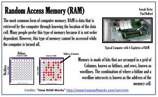
Picture of memory • You can think of computer memory as being one big array of data. • The address serves as an array index. • Each address refers to one word of data. • You can read or modify the data at any given memory address, just like you can read or modify the contents of an array at any given index. • If you’ve worked with pointers in C or C++, then you’ve already worked with memory addresses. Random Access Memory
2k x n memory ADRS OUT DATACS WR k n n Block diagram of RAM • This block diagram introduces the main interface to RAM. • A Chip Select, CS, enables or disables the RAM. • ADRS specifies the address or location to read from or write to. • WR selects between reading from or writing to the memory. • To readfrom memory, WR should be set to 0. OUT will be the n-bit value stored at ADRS. • To write to memory, we set WR = 1. DATA is the n-bit value to save in memory. • This interface makes it easy to combine RAMs together, as we’ll see. Random Access Memory
2k x n memory ADRS OUT DATACS WR k n n Memory sizes • We refer to this as a 2k x n memory. • There are k address lines, which can specify one of 2k addresses. • Each address contains an n-bit word. • For example, a 224 x 16 RAM contains 224 = 16M words, each 16 bits long. • The RAM would need 24 address lines. • The total storage capacity is 224 x 16 = 228 bits. Random Access Memory
Size matters! • Memory sizes are usually specified in numbers of bytes (8 bits). • The 228-bit memory on the previous page translates into: 228 bits / 8 bits per byte = 225 bytes • With the abbreviations below, this is equivalent to 32 megabytes. • To confuse you, RAM size is measured in base 2 units, while hard drive size is measured in base 10 units. • In this class, we’ll only concern ourselves with the base 2 units. Random Access Memory
Typical memory sizes • Some typical memory capacities: • PCs usually come with 512MB – 2GB RAM. • PDAs have 16-64MB of memory. • Digital cameras and MP3 players can have 32MB-8GB or more of onboard storage. • Many operating systems implement virtual memory, which makes the memory seem larger than it really is. • Most systems allow up to 32-bit addresses. This works out to 232, or about four billion, different possible addresses. • With a data size of one byte, the result is apparently a 4GB memory! • The operating system uses hard disk space as a substitute for “real” memory. Random Access Memory
2k x n memory ADRS OUT DATACS WR k n n Reading RAM • To read from this RAM, the controlling circuit must: • Enable the chip by ensuring CS = 1. • Select the read operation, by setting WR = 0. • Send the desired address to the ADRS input. • The contents of that address appear on OUT after a little while. • Notice that the DATA input is unused for read operations. Random Access Memory
2k x n memory ADRS OUT DATACS WR k n n Writing RAM • To write to this RAM, you need to: • Enable the chip by setting CS = 1. • Select the write operation, by setting WR = 1. • Send the desired address to the ADRS input. • Send the word to store to the DATA input. • The output OUT is not needed for memory write operations. Random Access Memory
Static memory • How can you implement the memory chip? • There are many different kinds of RAM. • We’ll start off discussing static memory, which is most commonly used in caches and video cards. • Later wemention a little about dynamic memory, which forms the bulk of a computer’s main memory. • Static memory is modeled using one latch for each bit of storage. • Why use latches instead of flip flops? • A latch can be made with only two NAND or two NOR gates, but a flip-flop requires at least twice that much hardware. • In general, smaller is faster, cheaper and requires less power. • The tradeoff is that getting the timing exactly right is a pain. Random Access Memory
Starting with latches • To start, we can use one latch to store each bit. A one-bit RAM cell is shown here. • Since this is just a one-bit memory, an ADRS input is not needed. • Writing to the RAM cell: • When CS = 1 and WR = 1, the latch control input will be 1. • The DATA input is thus saved in the D latch. • Reading from the RAM cell and maintaining the current contents: • When CS = 0 or when WR = 0, the latch control input is also 0, so the latch just maintains its present state. • The current latch contents will appear on OUT. Random Access Memory
My first RAM • We can use these cells to make a 4 x 1 RAM. • Since there are four words, ADRS is two bits. • Each word is only one bit, so DATA and OUT are one bit each. • Word selection is done with a decoder attached to the CS inputs of the RAM cells. Only one cell can be read or written at a time. • Notice that the outputs are connected together with a single line! Random Access Memory
The “C” in LogicWorks means “conflict.” Connecting outputs together • In normal practice, it’s bad to connect outputs together. If the outputs have different values, then a conflict arises. • The standard way to “combine” outputs is to use OR gates or muxes. • This can get expensive, with many wires and gates with large fan-ins. Random Access Memory
Those funny triangles • The triangle represents a three-state buffer. • Unlike regular logic gates, the output can be one of three different possibilities, as shown in the table. • “Disconnected” means no output appears at all, in which case it’s safe to connect OUT to another output signal. • The disconnected value is also sometimes called high impedance or Hi-Z. Random Access Memory
Connecting three-state buffers together • You can connect several three-state buffer outputs together if you can guarantee that only one of them is enabled at any time. • The easiest way to do this is to use a decoder! • If the decoder is disabled, then all the three-state buffers will appear to be disconnected, and OUT will also appear disconnected. • If the decoder is enabled, then exactly one of its outputs will be true, so only one of the tri-state buffers will be connected and produce an output. • The net result is we can save some wire and gate costs. We also get a little more flexibility in putting circuits together. Random Access Memory
Bigger and better • Here is the 4 x 1 RAM once again. • How can we make a “wider” memory with more bits per word, like maybe a 4 x 4 RAM? • Duplicate the stuff in the blue box! Random Access Memory
A 4 x 4 RAM • DATA and OUT are now each four bits long, so you can read and write four-bit words. Random Access Memory
16 8 8 Bigger RAMs from smaller RAMs • We can use small RAMs as building blocks for making larger memories, by following the same principles as in the previous examples. • As an example, suppose we have some 64K x 8 RAMs to start with: • 64K = 26 x 210 = 216, so there are 16 address lines. • There are 8 data lines. Random Access Memory
Making a larger memory • We can put four 64K x 8 chips together to make a 256K x 8 memory. • For 256K words, we need ?? address lines. Random Access Memory
8 16 8 Making a larger memory • We can put four 64K x 8 chips together to make a 256K x 8 memory. • For 256K words, we need 18 address lines. • The two most significant address lines go to the decoder, which selects one of the four 64K x 8 RAM chips. • The other 16 address lines are shared by the 64K x 8 chips. • The 64K x 8 chips also share WR and DATA inputs. • This assumes the 64K x 8 chips have three-state outputs. Random Access Memory
8 16 8 Analyzing the 256K x 8 RAM • There are 256K words of memory, spread out among the four smaller 64K x 8 RAM chips. • When the two most significant bits of the address are 00, the bottom RAM chip is selected. It holds data for the first 64K addresses. • The next chip up is enabled when the address starts with 01. It holds data for the second 64K addresses. • The third chip up holds data for the next 64K addresses. • The final chip contains the data of the final 64K addresses. Random Access Memory
8 16 11 1111 1111 1111 1111 (0x3ffff) to 11 0000 0000 0000 0000 (0x30000) 10 1111 1111 1111 1111 (0x2ffff) to 10 0000 0000 0000 0000 (0x20000) 01 1111 1111 1111 1111 (0x1ffff) to 01 0000 0000 0000 0000 (0x10000) 00 1111 1111 1111 1111 (0x0ffff) to 00 0000 0000 0000 0000 (0x00000) 8 Address ranges Random Access Memory
Making a wider memory • You can also combine smaller chips to make wider memories, with the same number of addresses but more bits per word. • How do we create a 64K x 16 RAM from two 64K x 8 chips? Random Access Memory
8 8 16 8 8 Making a wider memory • You can also combine smaller chips to make wider memories, with the same number of addresses but more bits per word. • Here is a 64K x 16 RAM, created from two 64K x 8 chips. • The left chip contains the most significant 8 bits of the data. • The right chip contains the lower 8 bits of the data. Random Access Memory
Summary • A RAM looks like a bunch of registers connected together, allowing users to select a particular address to read or write. • Much of the hardware in memory chips supports this selection process: • Chip select inputs • Decoders • Tri-state buffers • By providing a general interface, it’s easy to connect RAMs together to make “longer” and “wider” memories. • Next, we’ll look at some other types of memories • We now have all the components we need to build our simple processor. Random Access Memory