Download
1 / 10
100 likes | 200 Vues
Card being developped at Université de Montréal for the KOPIO collaboration at Brookhaven National Laboratory (intended for the readout of the pre-radiator cathode strips; 100,000 channels) FEATURES: - Prototype version has VME interface => suitable for various test systems

E N D
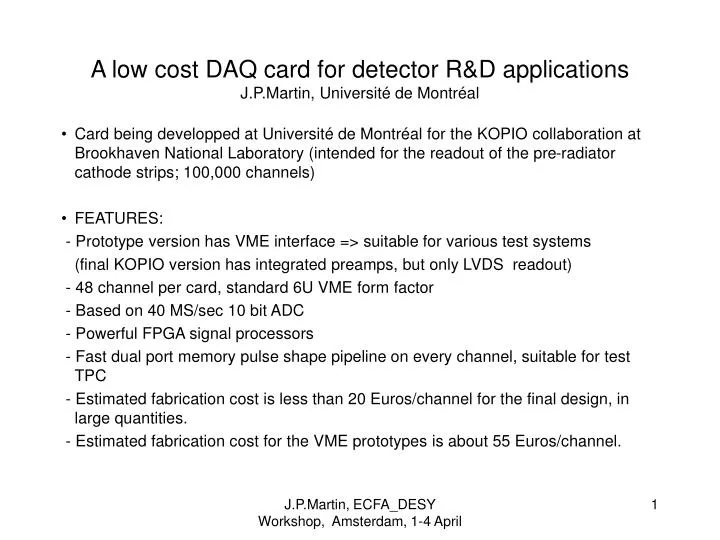
Card being developped at Université de Montréal for the KOPIO collaboration at Brookhaven National Laboratory (intended for the readout of the pre-radiator cathode strips; 100,000 channels) FEATURES: - Prototype version has VME interface => suitable for various test systems (final KOPIO version has integrated preamps, but only LVDS readout) - 48 channel per card, standard 6U VME form factor - Based on 40 MS/sec 10 bit ADC - Powerful FPGA signal processors - Fast dual port memory pulse shape pipeline on every channel, suitable for test TPC - Estimated fabrication cost is less than 20 Euros/channel for the final design, in large quantities. - Estimated fabrication cost for the VME prototypes is about 55 Euros/channel. A low cost DAQ card for detector R&D applicationsJ.P.Martin, Université de Montréal J.P.Martin, ECFA_DESY Workshop, Amsterdam, 1-4 April
I n p u t c o n n e v t o r (48 pairs) KOPIO DAQ card architecture 300 MBauds serial interface LVDS lines (4) RJ45 Differential amplifier Low pass filter 8 channels 40 MS/sec 10 bit FADC ALTERA Cyclone FPGA 1 Trigger 1 Differential amplifier Low pass filter 2 Cable from preamps Event collector, VME interface . . . . . . . . . . . . . . 8 channel 40 MS/sec 10 bit FADC ALTERA Cyclone FPGA Synchro 6 Differential amplifier Low pass filter 48 System clock J.P.Martin, ECFA_DESY Workshop, Amsterdam, 1-4 April
Data flow and processing in FPGA (one channel),(example for TPC pad readout application) Trigger window generator (up to 4 windows, overlap allowed.) Drift time Coarse resolving time LVDS Trigger Data segment accept logic Multi event buffer, capacity: 4 events Readout interface Accept VME Hit detector Time stamp generator Feature extraction logic Time vernier Amplitude Pulse shape segment Dual port circular latency buffer Parameters FADC bits Size: 3.2microseconds J.P.Martin, ECFA_DESY Workshop, Amsterdam, 1-4 April
Details of the data segment accept logic(one of 4 parallel channels) a Time stamp a>b a Accept window begin time b a-b Trigger window begin time Accept b a Accept window end time a+b a Coarse resolving time b a<b Hit detector time b a a<b Trigger window end time b J.P.Martin, ECFA_DESY Workshop, Amsterdam, 1-4 April
Details of the feature extraction (example) Accept signal FADC bits Digital triangular filter Peak detector Amplitude of filtered peak Above threshold Digital differentiator Negative values suppressor Centroid evaluator Linearisation function Time vernier FADC data gate Pulse shape data Time stamp (clock counter) J.P.Martin, ECFA_DESY Workshop, Amsterdam, 1-4 April
QUARTUS II top level diagram of KOPIO digital filters J.P.Martin, ECFA_DESY Workshop, Amsterdam, 1-4 April
KOPIO flat top digital filter, QUARTUS II diagram J.P.Martin, ECFA_DESY Workshop, Amsterdam, 1-4 April
Preliminary specifications for a TCP readout application • Analog inputs: 48 differential pairs, 100 ohms impedance, flat cable or twisted pairs, 100 pin fine pitch (0.025”) connector • Dynamic range: 1000:1 • Analog dynamic range of ADC: plus/minus 0.5 volts • Analog gain before ADC: fixed between 2 and 20 according to requirement, DC coupled • Maximum pulse shape sampling frequency: 40 MHz • Low pass filter cutoff frequency, <1/2 sampling frequency • Timing resolution: <5 nanoseconds with 20:1 S/N ratio • Trigger rate: limited by readout system throughput: • - For VME, reading out only the time and amplitudes, 20 • modules in a crate, about 15 KHz; • full pulse shape readout, 960 channels, 100 samples: 10 Hz • with zero suppression: scales according to occupancy • -For LVDS, one to 20 times faster, according to the readout • of the LVDS data collector modules, assumong no processing • in the collector modules J.P.Martin, ECFA_DESY Workshop, Amsterdam, 1-4 April
Picture of the PCB at the current stage of development J.P.Martin, ECFA_DESY Workshop, Amsterdam, 1-4 April
Milestones • Completion of the PCB routing: 30 April 2003 • Delivery of the PCB bare boards: 15May 2003 • First prototype manually populated and electrically tested: 3 rd week of June 2003 • Prototype working with the minimal KOPIO firmware: mid July 2003 • Refinement of KOPIO firmware completed: mid August • Modifications for other applications (i.e. TPC) : starting mid August J.P.Martin, ECFA_DESY Workshop, Amsterdam, 1-4 April