Download
1 / 20
200 likes | 203 Vues
This presentation discusses the proposal for the electronics and trigger architecture of the SuperB experiment, based on the experience of the BABAR detector and LHC experiments. It highlights the main elements of the system, including the Fast Control and Timing System (FCTS), Common Front-End Electronics (CFEE), L1 hardware trigger (L1T), Read-Out Module (ROM), and Experiment Control System (ECS).

E N D
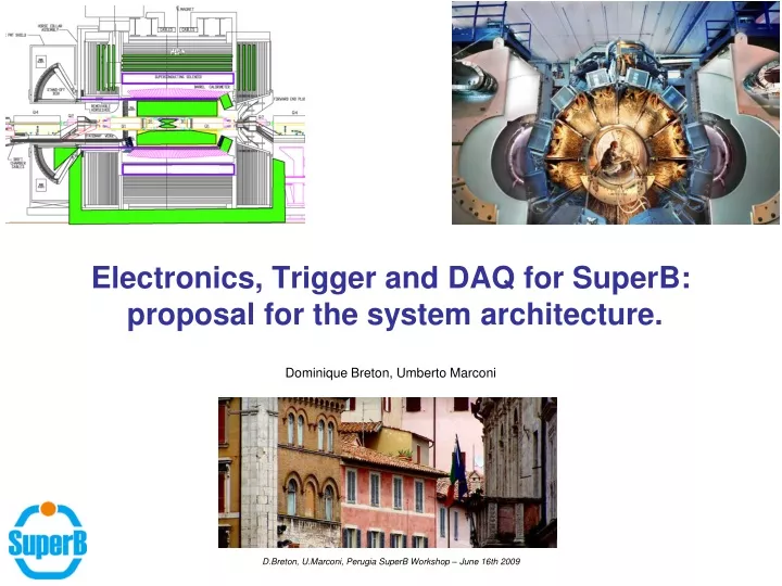
Electronics, Trigger and DAQ for SuperB: proposal for the system architecture. Dominique Breton, Umberto Marconi D.Breton, U.Marconi, Perugia SuperB Workshop – June 16th 2009
Electronics, trigger and DAQ architecture. • Editors: D. Breton (LAL Orsay) and U. Marconi (INFN Bologna). • This presentation aims at summarizing the document sent to the collaboration in early June 2009 and proposing a base for the electronics architecture of the experiment. • It is based on the experience acquired both on building, commissioning, running and maintaining over a long term the BABAR detector and on building and commissioning the LHC experiments. • For its writing, we got the fruitful help of: J. Maalmi (LAL), C. Beigbeder (LAL), D. Charlet (LAL), D. Galli (Bologna University/INFN). • During its preparation, numerous meetings with experts of the domain have been held. We especially wish to thank: Beat Jost and Richard Jacobsson from CERN. • In preparation of this document, we had several discussions with colleagues from SuperB we wish to thank: M. Bellato (INFN), A. Aloisio (INFN) D.Breton, U.Marconi, Perugia SuperB Workshop – June 16th 2009
Introduction • The main goal is to design the simplest reliable system able to fulfil the requirements, including wide enough safety margins. • Said requirements have been described in the document released in February 2009 for the Orsay workshop. • As it was evoked many times since the work started on these subjects, we proposed that the architecture of SuperB electronics evolves from that of BABAR experience, actually getting closer to that of LHC experiments. This is mainly due to three factors: • The large upgrade of the requirements; • The evolution of the technologies; • The potential radiation level on the detector. • The main elements of the system presented in this document, as they are visible on the next page, are the following: • The Fast Control and Timing System (FCTS); • The Common part of Front-End Electronics (CFEE) for data read-out, configuration and control; • The L1 hardware trigger (L1T); • The Read-Out Module board (ROM); • The Experiment Control System (ECS). D.Breton, U.Marconi, Perugia SuperB Workshop – June 16th 2009
Overall system architecture proposal D.Breton, U.Marconi, Perugia SuperB Workshop – June 16th 2009
Introductory remarks • We decided to separate the different links in order to simplify the building of the system. • Having all the main functions (FCTS, ECS, Readout) grouped in the same link like in BABAR makes it difficult to: • design the ROM which concentrates all the critical items • rapidly deliver boards for subdetector test benches • debug the system • Conversely, having separate links permits developing the different systems independently and providing them to the subdedector FEE teams as soon as they are available. • In particular, having a dedicated ECS link permits an easy independent commissioning of the different subdetectors. • A backup clock has to be provided in case of failure of the FCTS system, thus always keeping the link to the detector alive • We think that making use of commercial components as much as possible would allow us to set up a more aggressive schedule • Anyway, at this given time, there is no certitude that every field can be covered that way. D.Breton, U.Marconi, Perugia SuperB Workshop – June 16th 2009
The FCTS system • The Fast Control and Timing System (FCTS) of SuperB is in charge of managing all the elements linked to the clock, trigger and event readout. • It is also in charge of the partitioning of the detector in independent sub-systems for testing and commissioning purposes. • necessary to make use of two dedicated switches: • delivering the clock and commands to the FEE; • collecting the throttling requests back from ROM or ECS system; • implemented on dedicated boards. • The main board of the system is the Fast Control and Timing Module (FCTM), in charge of managing the main FCTS functions. • The FCTS system will be implemented in a crate with a custom backplane • point to point distribution of all the necessary signals • very clean synchronous signals • almost no bothering cables. • The FCTM should include all functionalities which allow it to be present in the FCTS crate in as many instances as the number of partitions needed. • One given FCTM could be dedicated to the unused subsystems. • It is too slow to throttle the L1 rate directly from the front-end electronics • => models of the L1 buffer event queues will be emulated inside the FCTM in order to deliver an instantaneous throttling in case of need. D.Breton, U.Marconi, Perugia SuperB Workshop – June 16th 2009
Architecture of the FCTS for the fast control D.Breton, U.Marconi, Perugia SuperB Workshop – June 16th 2009
Block diagram of the FCTM board • The Fast Control and Timing Module (FCTM) is in charge of managing the following functions: • Synchronizing the experiment with the machine; • Delivering and buffering the clock to the experiment; • Dealing with the raw L1 trigger decisions; • Throttling the latter if necessary; • Generating widely programmable local triggers for calibration and commissioning; • Generating calibration pulses; • Generating all the synchronous reset commands; • Producing the BxID and event ID; • Managing the stack of IP addresses of the farm PCs and broadcasting them; • Keeping a trace of all event-linked data to be put in the event readout. D.Breton, U.Marconi, Perugia SuperB Workshop – June 16th 2009
Farm IP address management • The FCTM has to manage the IP addresses of the farm PCs to distribute the Multi-Event Packets (MEP) to the farm. • This can be implemented either in firmware or in software on the board. • Free PCs inform the FCTM of their availability through Ethernet requests containing information about their computing capacity (“credits”). • Then the address used for the next MEP (or a subset of it to limit the bandwidth necessary) has to be sent to the ROMs. • This can be done either: • through the FCTS links => naturally synchronizes the closure of the MEPs with the L1 commands • through an Ethernet broadcast. • In the same manner, a firmware implementation of the address management would allow it to be treated synchronously with said L1 commands. • Even with a solution based on the available capacity of the PC farm, throttling might be necessary. • In order to restore the events truncated in the FEE because of pile-up, two solutions can be envisaged for the restoration: • It takes place in the ROM => the FCTM does not have any constraints to close the MEPs. • It takes place in the PC farm => the FCTM has to close the MEPs only if there is no data overlap in the last treated trigger. D.Breton, U.Marconi, Perugia SuperB Workshop – June 16th 2009
Common Front-end electronics • It would be wise to separate the functions required to drive the front-end electronics by using dedicated independent elements for the implementation of the different functionalities. • These elements could be implemented as mezzanines or as circuits directly mounted on the front-end modules (considered here as carrier boards). • One mezzanine should be used for FCTS signals and commands decoding, • Another one for the ECS management. • Both could be merged to optimize the integration • It could also appear useful to decode the FCTS and ECS signals on their mezzanine and to distribute them to the neighbouring boards. • Driving of L1 buffers may also be managed by a dedicated control circuitry, which may be actually implemented inside a radiation tolerant FPGA. • The L1 buffers should sit on the carrier boards and leave to the control circuitry the sole management of the commands and of the event buffer transmission. • Serializers and link optical drivers should also sit on the carrier boards, this mainly for mechanical and thermal reasons. D.Breton, U.Marconi, Perugia SuperB Workshop – June 16th 2009
The front-end buffers and control circuitry • The control circuitry would have to: • handle the L1 accept commands and to provide the signals necessary to control the reading of the latency buffer and the writing/transmitting of the proper event buffer. • deal with the potential pile-up of events and the possibility to go back in time after a rejected Bhabha event for the concerned sub-detectors (in case said rejection were implemented), without forgetting the handling of the fast multiplexer feeding the optical link serializer. D.Breton, U.Marconi, Perugia SuperB Workshop – June 16th 2009
L1 Trigger • L1 Trigger will be built as a synchronous machine running at 56MHZ, based on primitives produced by dedicated electronics located on the front-end boards or any other dedicated boards in charge of the concerned sub-detectors. It will be divided into three main elements: • The Drift Chamber processor • The Electromagnetic calorimeter processor. • The Global Trigger Processor, combining both others. • Baseline implementation of the L1 trigger => the BABAR L1 architecture • could be extended to add in case the SVT trigger and Bhabha veto. • The standard chosen for the crates might probably move to ATCA crate and backplane. On the other hand, the boards might be full custom. • Main goal => considerably reduce the trigger latency (about 12µs in BABAR). • Said latency indeed directly impacts the size of L1 data buffers in the FEE. • Also try if possible to improve the event time precision, but the latter is mostly linked to the precision of the trigger primitives produced in the FEE. • The L1 trigger raw output will be sent to the FCTM boards which will then forward it after a possible throttling towards the whole experiment. D.Breton, U.Marconi, Perugia SuperB Workshop – June 16th 2009
Read Out Module • The ROM design is standard for all sub-detectors but is flexible in use <= based on FPGAs. • It is in charge of interfacing the front-end electronics with the DAQ system. It provides: • zero suppression, • feature extraction, • data formatting, • and a large network interface buffer. • Therestoration of the event data truncated in the FEE because of pile-up can be: • performed by the PC farm • => smaller size of the buffers in the ROM, smaller network bandwidth • => but larger processing load in the PCs. • performed by the ROM • => lighter architecture but larger buffers and possible throttling if pile-up lasts too long. • Throttling of L1 trigger is directly performed through binary signals. • The event number will be used to associate the event to the IP address of the next available PC. Said address will either be broadcasted by the FCTM through Ethernet, or rather through the FCTS links, then permitting the MEP closure at the same time. D.Breton, U.Marconi, Perugia SuperB Workshop – June 16th 2009
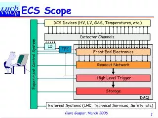
Experiment Control System (1) • The complete SuperB experiment (magnet, power supplies, front-end, DAQ, etc.) must be accessible through the control of ECS. • The ECS system will be responsible for the overall control of the experiment and the monitoring of its correct functioning. In particular, ECS is in charge of: • Setting up and reading back the different registers and memories located on the experiment; • Allowing the calibration and test of the front-end electronics; • Monitoring the status of the readout chain; • Reading events during commissioning and spying them if wanted during runs. • Numerous front-end parameters must be initialized to specific values before the system is capable of working correctly. • In some cases: only a few parameters per detector channel/group of channels. • In other cases: individual lookup tables for each channel. • The loading of the front-end parameters needs in principal not to be performed frequently when the system is working reliably. • In the case of front-end electronics located in a hostile environment it may be required to frequently reload the parameters to ensure that the local registers storing said parameters have not been corrupted by SEUs. • As it is difficult to estimate the order of magnitude of this problem, it is important to construct the front-end hardware in such a way that no critical bottlenecks exists in the architecture of the ECS system. D.Breton, U.Marconi, Perugia SuperB Workshop – June 16th 2009
ECS in the overall system D.Breton, U.Marconi, Perugia SuperB Workshop – June 16th 2009
Experiment Control System (2) • It is important that the bandwidth requirements to the ECS system for loading the front-end parameters are specified (estimated) as early as possible to enable the architecture of the ECS system to handle the specific requirements of all sub-detectors. • Ethernet will be used for ECS communication off-detector. • During calibration runs an extended functionality of the ECS system will be required. • The specific requirements to the ECS system during calibration runs must be specified as early as possible by each sub-detector. • An important role of the ECS system is to continuously monitor the correct function of the experiment. • For security reason, an independent Detector Safety System (DSS) has to protect the experiment against major damage to equipment in case the software-based ECS system is not running correctly. • For the FEE, the protection system must monitor the correct function of power supplies (over-voltage, over-current, etc…) and the cooling of electronic crates (temperature sensors). • Monitoring of the correct function of front-end modules during operation must to a large extent be built into the front-end. • When some malfunction is detected, the front-end must inform the ECS system about the failure. D.Breton, U.Marconi, Perugia SuperB Workshop – June 16th 2009
Experiment Control System (3) • The ECS system must also be capable of performing exhaustive tests of individual modules while they are located in the system (in-situ). • The ideal case: each module can perform a self-test initialized by the ECS and a simple status will indicate the result (difficult and expensive). • Alternatively the test of modules can be performed by an external controller processor (not great in a harsh environment). • The easiest: the test of a module will be driven directly by the ECS system • => this requires extensive software routines • => The development of these software test routines must be considered an integral part of the development of the module itself as its functions requires detailed knowledge about the implementation of the module. • The field bus used for ECS has to be radiation tolerant on its detector side, and to ensure a very high reliability. • Such a bus has been designed for LHCb experiment: it is called SPECS (as Serial Protocol for Experiment Control System). • This bidirectional 10Mbit/s bus runs over standard Ethernet Cat5+ cable and provides all possible facilities for ECS on a small mezzanine. It could be easily adapted to the SuperB requirements. • SPECS which was initially based on PCI boards is currently being translated to an Ethernet-based system also integrating all the functionalities for the out-of-detector elements. D.Breton, U.Marconi, Perugia SuperB Workshop – June 16th 2009
Fast links • The main difficulty was most that commercial chipsets where data and clock are embedded together do not guaranty a constant latency of the decoded data (inside a clock period) and a constant phase of the extracted clock at each power-up. Yet, this is a strict requirement for our system, in addition to a low jitter for the clock. • For the ROM link, solutions based on standard FPGA can be further studied. But as already evoked, the radiation environment makes the problem more difficult to solve for the FEE side, namely the Rx part of the FE link and the Tx part of the Readout link. • R&D work has started on these links and chipsets are being tested. • Backup solutions making use of two links, one of them carrying the clock, and the second one the serialized commands look feasible. • The common requirements will be to be based on commercial components and to be easy to implement and work out, and to be fully reliable. D.Breton, U.Marconi, Perugia SuperB Workshop – June 16th 2009
Miscellaneous • Dataflow control: • Counters have to be mounted all along the control and data chain to check for consistency of dataflow with the central system. • It is for instance very useful for commissioning and monitoring to know how many triggers or calibration commands passed at different locations and how many consecutive events were sent. • A dedicated command (“Snapshot”) should be implemented in the FCTS to copy the status of all these counters at the detector scale at a given synchronous time into registers accessible through ECS. • Power and ground: • Ground has to be as equipotential as possible. This begins as soon as when building the experiment hall, were it would be wise to foresee the possibility to connect the iron bars sunken in the concrete ground to the experiment electrical ground, in order to provide the most perfect possible mesh. • Power supplies should if possible remain outside of the radiation area, because radiation tolerant power supplies are expensive and less reliable. Therefore, power consumption on the detector has to remain reasonable, in order to limit the power loss along the cables. D.Breton, U.Marconi, Perugia SuperB Workshop – June 16th 2009
Conclusion • This presentation and the document it refers to describe the base of the architecture we want to set up for SuperB, and will be the template used for the white paper and then for the TDR. • It is however not frozen yet. • A few remarks: • We need a precise estimation of the window lentgh, data rates and number of links for all the sub-detectors, in order to be able to scale the system, and to optimize its topology. • This proposal is based on L1 buffers located in the FEE, but options where the latter would be moved farther in the dataflow chain will still be studied (data driven models => link cost ? ). • Validating commercial components for the implementation of high speed optical links is on tracks in order to provide a solid proposal for the TDR. • All the other elements in the architecture (FCTS, ROM, ECS) are currently covered for the TDR, except the level 1 trigger. D.Breton, U.Marconi, Perugia SuperB Workshop – June 16th 2009