Download
1 / 21
330 likes | 734 Vues
What is Thin Film Deposition?. Ms. Crystal J. Woods Emmett J. Conrad STEM Academy High School Dallas, TX. Dr. Haiyan Wang, Assistant Professor, Electrical and Computer Engineering. Education Ph.D., North Carolina State University, Raleigh, NC, 2002

E N D
What is Thin Film Deposition? Ms. Crystal J. Woods Emmett J. Conrad STEM Academy High School Dallas, TX
Dr. Haiyan Wang, Assistant Professor, Electrical and Computer Engineering Education • Ph.D., North Carolina State University, Raleigh, NC, 2002 • M.S., Institute of Metal Research, Shenyang, China, 1999 • B.S., Nanchang University, Nanchang, China, 1998 Previous Appointments • Jan.05-Dec.05 - Technical Staff Member, Los Alamos National Laboratory • Jan.03-Dec.04 - Director Funded Postdoctoral Fellow, Los Alamos National Laboratory Research Interests • Nanostructured nitride and oxide thin film heterostructures for microelectronics, optoelectronics, magnetic, high temperature superconductors, solid oxide fuel cells, radiation tolerance and structural applications; • High temperature superconductors: coated superconductor scale-up and architectures; flux-pinning mechanisms of nanoparticles and defects • Microstructural characterizations with transmission electron microscopy (TEM), high resolution TEM, Scanning transmission electron microscopy (STEM) and XRD. Patents • 8 patents in the areas of thin film architecture and high temperature superconductors • Selected journal publications (105 journal articles and 70 conference proceedings and presentations by January 2008) • H. Wang, R. Araujo J.G. Swadener, Yongqiang Wang, X. Zhang, E. G. Fu and T. CaginIon Irradiation Effects in Nanocrystalline TiN Coatings, Nuclear Instruments
E3 Research Topic: Thin Film Deposition (Growth) w/ Dr. Wang • Dr. Haiyan Wang, Assistant Professor, Electrical and Computer Engineering, TAMU • David Mortimer, Physics Teacher, Del Rio High School • Crystal J. Woods, Algebra Teacher, Emmett J. Conrad STEM Academy High School
Use of Thin Film Deposition • Thin Film Growth or Deposition: It is a thin layer of coating on a substrate or template. It serves one or multiple physical purposes including protection, decoration, conducting, reflection, data storage, insulation, etc. • Examples: Colorful coatings on cars, golden watches and many others; • Corrosion resistive coatings and superhard coatings (petroleum industry, chemical factories, etc.); • Semiconductor industry (Pentium processors, microchips, memories, iPod, etc.); • “Sunscreen” : a protective coating on your skin.
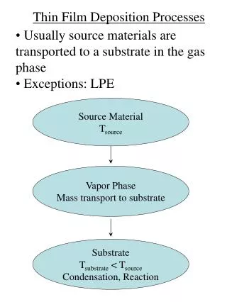
Thin Film: How does it grow? • Kinetic Energy of molecules impact the growth of Thin Film. • Pressure affects the momentum of the molecules. • The energy of the molecules impacts how the molecules find their way to the target, so they can form layers. • The following Parameters will result in a desired epitaxial layer (organized, carefully placed, high quality layer of thin film): Temperature Pressure Laser Energy Laser Frequency Type of material (Metals) Type of Substrate (Base layer: Metal or Ceramic)
Understanding Thin Film Growth • Dr. Wang explains thin film growth as “laying of apples” • A high quality thin film growth must be layered in an organized pattern. Molecules must be laid on the target in non-disruptive pattern. • No traffic jams, “no rush hour” free flowing traffic. High Quality Growth: • Ordered foundation • Same size • Same pattern • Right time • Right condition
Understanding Thin Film Growth • Atoms must be able to move around on the substrate until they find the right spot. This results in the growth layer.
Understanding Thin Film Growth • Congruency is a key component of thin film growth. • Similar shapes and/or congruent shapes prevents gaps or defects in growth layers.
Summer Research: My Exposure of Thin Film Joon Hwan Lee, Ph.D. Candidate Research: Transmittance of Light within Thin Film Tools: Spectrophometer, measures transparency of material using wavelengths. Wavelengths are used to determine absorption of life. Focus: Compare/Contrast Transmittance when Parameters have been altered
Summer Research: My Exposure of Thin Film Jie (Joyce) Wang, Ph.D. Candidate Research: High Temperature Superconductor Tools: Transmission Electron Microscopy, JEOL JEM-2010 (TEM) Focus: Compare/Contrast Attachment Layer of Growth when temperature has been changed . The key is to find nice layers of growth.
Summer Research: My Exposure of Thin Film Zhenxing Bi, Ph.D. Candidate Research: Growth of Vertical Patterns of Thin Film Tools: Transmission Electron Microscopy, JEOL JEM-2010 (TEM) Focus: Compare/Contrast Thickness and/or Mircostructural Changes when Parameters have been changed. Goal to create high quality vertical patterns.
My experience of Thin Film Research • Designing a high quality thin film growth that demonstrates an organized pattern of the same and/or similar shape with various parameters. • Continue exploring results when different parameters of the thin film process have been changed.
E3 Summer Research Program Ms. Woods @ TAMU’s E3 Summer Research Program High Quality Education
Thin Film vs. Algebra Patterns producing: High Quality thin film growth Equations Linear Functions Exponential Functions Scatter Plots Quadratic Functions Factoring Ordered foundation Same size Same pattern Right time Right condition
Examples of Patterns in Algebra • The powers of 11 also form a sequence: • 110 = 1111 = 11112 = 121113 = 1331114 = 14641115 = 161051116 = 1771561117 = 19487171
Using Patterns of Tiles with Quadratic Functions and Factoring
Data Used to create Functions Exponential Functions Linear Functions
Kudos! to my wonderful Thin Film Research Team Big Thanks to the National Science Foundation! Ick-Chan Kim, Ph.D. Candidate Roy Araujo, Ph.D. Candidate Jongsik Yoon, Ph.D. Candidate Joon Hwan Lee, MS Candidate Harrison Tsai, MS Candidate Jie (Joyce) Wang, Ph.D. Candidate Zhenxing Bi, Ph.D. Candidate Sungmee Cho, Ph.D Candidate Dr. Haiyan Wang