Download
1 / 24
240 likes | 420 Vues
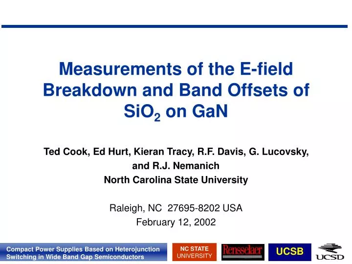
Measurements of the E-field Breakdown and Band Offsets of SiO 2 on GaN. Ted Cook, Ed Hurt, Kieran Tracy, R.F. Davis, G. Lucovsky, and R.J. Nemanich North Carolina State University Raleigh, NC 27695-8202 USA February 12, 2002. Introduction.

E N D
Measurements of the E-field Breakdown and Band Offsets of SiO2 on GaN Ted Cook, Ed Hurt, Kieran Tracy, R.F. Davis, G. Lucovsky, and R.J. Nemanich North Carolina State University Raleigh, NC 27695-8202 USA February 12, 2002
Introduction • The band offsets have a direct effect on the properties of the interface, and therefore affect the reliability and stability of the device • Investigation of the band offsets, as well as their effects, such as E-field breakdown, is important for device fabrication, and will be explored in this study
Goal and Motivation Goal: • Measure the Valence Band Offsets between atomically clean GaN and SiO2 using photoemission techniques Motivation: • Passivation of high voltage devices • Wafer Bonding – fusion bonded interfaces • Gate insulator applications
Experimental Procedure • Achieve atomically clean GaN surface using CVC anneal in NH3 atmosphere @ 860°C for 15 minutes • XPS and UPS performed after each of the following steps to track the evolution of peak shifts • Deposition of 2Å Si via MBE • Deposition of a second 2Å Si layer • Oxidation of Si layer using a Remote O2 plasma • Deposition of 2Å, and oxidation of the Si layer • 650°C anneal for 15 minutes to densify the oxide • Deposition of 3Å, and oxidation of the Silicon layer • Final anneal at 650°C for densification
Integrated UHV Surface and Interface Processing System LoadLock Field Emission ECR N2 Plasma Wafer Bonding Si-Ge MBE ARUPS XPS GSMBE High Voltage Testing CVD Diamond AES / LEED e-beam evap Hydrogen/Oxygen Plasma
Proposed Valence Band Line-up between n-GaN and SiO2 6.0 Ef 5.5 Ec 5.0 Ev 4.5 c = 1.1eV Evac 4.0 3.5 3.0 2.5 Ec-Ef = 3.70eV 2.0 c = 2.9eV D Ec = 3.6eV 1.5 1.0 Ec-Ef =0.08eV 0.5 0.0 Eg = 9.0eV -0.5 -1.0 Ed = 0.3eV -1.5 E g = 3.40eV Ef-Ev = 3.32eV -2.0 Ef-Ev = 5.30eV -2.5 -3.0 -3.5 -4.0 D Ev = 2.0eV -4.5 -5.0 -5.5 GaN SiO2 -6.0 Clean
Energy Band Diagram CB CB Ef Ef VB VB Clean GaN Surface Final Surface
UPS Spectra of VB turn-on 0.3 eV shift due to band bending
Valence Band Offset between GaN and SiO2 6.0 Ef 5.5 Ec 5.0 Ev 4.5 c = 1.1eV Evac 4.0 3.5 3.0 2.5 Ec-Ef = 3.70eV 2.0 c = 2.9eV D Ec = 3.6eV 1.5 1.0 Ec-Ef =0.08eV 0.5 0.0 Eg = 9.0eV -0.5 -1.0 Ed = 0.3eV -1.5 E g = 3.40eV Ef-Ev = 3.32eV -2.0 Ef-Ev = 5.30eV -2.5 -3.0 -3.5 -4.0 D Ev = 2.0eV -4.5 -5.0 -5.5 GaN SiO2 -6.0 Clean
UPS Spectra of Spectral Width W=11.1 eV Eg SiO2 =9.0 eV c=21.2-11.1-9.0 = 1.1 eV c=hn-W-Eg c=21.2-14.9-3.4 = 2.9 eV Eg GaN =3.4 eV W=14.9 eV
Electron Affinity difference between GaN and SiO2 6.0 Ef 5.5 Ec 5.0 Ev 4.5 c = 1.1eV Evac 4.0 3.5 3.0 2.5 Ec-Ef = 3.70eV 2.0 c = 2.9eV D Ec = 3.6eV 1.5 1.0 Ec-Ef =0.08eV 0.5 0.0 Eg = 9.0eV -0.5 -1.0 Ed = 0.3eV -1.5 E g = 3.40eV Ef-Ev = 3.32eV -2.0 Ef-Ev = 5.30eV -2.5 -3.0 -3.5 -4.0 D Ev = 2.0eV -4.5 -5.0 -5.5 GaN SiO2 -6.0 Clean
Models of Heterojunctions EAM IDM • Electron Affinity Model Valid if small or no change in the interface Dipole • Interface Dipole Model Change in the Electric field at interface • Deviation from the electron affinity of the heterojunction alignment represents the interface dipole
Interface Dipole in Band Line-up of GaN and SiO2 6.0 Ef 5.5 Ec 5.0 Ev 4.5 c = 1.1eV Evac 4.0 3.5 3.0 2.5 Ec-Ef = 3.70eV 2.0 c = 2.9eV D Ec = 3.6eV 1.5 1.0 Ec-Ef =0.08eV 0.5 0.0 Eg = 9.0eV -0.5 -1.0 Ed = 0.3eV -1.5 E g = 3.40eV Ef-Ev = 3.32eV -2.0 Ef-Ev = 5.30eV -2.5 -3.0 -3.5 -4.0 D Ev = 2.0eV -4.5 -5.0 -5.5 GaN SiO2 -6.0 Clean D=1.9 eV
Conclusions for n-type experiment • Special care has been taken to prevent oxidation of gallium • Band bending of ~0.3 eV for CVC GaN surface • Electron Affinity ~2.9 eV for CVC GaN surface • Flat Bands at the GaN-SiO2 Interface • Valence Band Offset of ~2 eV for GaN-SiO2 for 1x1017cm-3 n-type GaN • Conduction Band offset of ~3.6 eV for GaN-SiO2 assuming EgSiO2 =9.0 eV • Deviation from the Electron Affinity model due to Interface dipole of ~1.9 eV
Proposed Valence Band Line-up between p-GaN and SiO2 6.0 Ef 5.5 Ec 5.0 Ev 4.5 Evac 4.0 3.5 3.0 2.5 Ec = 3.3eV Ec-Ef =3.1eV E = 3.40eV 2.0 g 1.5 Ec-Ef = 4.5eV 1.0 EB=0.3eV 0.5 0.0 -0.5 Eg = 9.0eV Ef-Ev = 4.5eV Ef-Ev=1.7eV -1.0 Ef-Ev = 2.2eV -1.5 -2.0 -2.5 -3.0 Ev = 2.3eV -3.5 -4.0 -4.5 -5.0 Clean GaN SiO2 -5.5 -6.0
Conclusions for p-type experiment • Initial Band Bending of 1.4 eV for CVC GaN surface • Additional downward Band Bending of ~0.5 eV as the surface was formed • Valence Band offset of ~2.3 eV for GaN-SiO2 for 2x1018 cm-3 p-type GaN • Conduction Band Offset of 3.3 eV for GaN-SiO2 assuming Eg Sio2 =9.0 eV
E-field Breakdown Procedure • Achieve atomically clean GaN surface using CVC anneal in NH3 atmosphere @ 860°C for 15 minutes • Deposit 4Å Si via MBE on surface to help prevent oxidation of the Gallium • Deposit 300Å SiO2 via Remote O2 Plasma • Anneal to 650°C to densify the oxide • Form 0.068 mm2 Al contacts on the surface using photolithographic techniques • Electrical characterization of sample
Device Structure for Electrical Testing Al Contacts V SiO2 GaN AlN SiC W Contact I CRT v
Breakdown Frequency 300Å SiO2 unintentionally doped, n-type <1.0x1017 cm-3
Conclusions • These high values of breakdown voltage lends to the notion that the GaN layer is having an insulating effect • A full understanding of this effect requires more study • Film deposition rate of 2.5 Å/min established; verified by ellipsometry and C-V measurements
Future Work • Reduce Band Bending for p-type GaN/SiO2 -Improve cleaning methods -Oxide integrity • Effect of different passivation layers • Si3N4 • High k dielectrics