Download
1 / 15
150 likes | 425 Vues
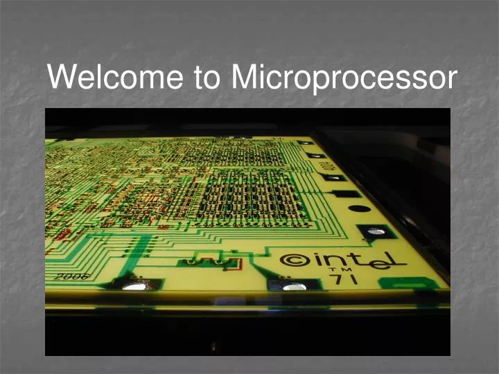
Welcome to Microprocessor. MICROPROCESSOR. DEFINITION. A microprocessor is a tiny piece of silicon with millions of microscopic Interconnected transistors etched onto it. This circuitry is divided into sections with specific functions, which together perform the task of most

E N D
MICROPROCESSOR DEFINITION A microprocessor is a tiny piece of silicon with millions of microscopic Interconnected transistors etched onto it. This circuitry is divided into sections with specific functions, which together perform the task of most electronic devices –from calculators to cell phones to supercomputer. While there are different types of microprocessors, they all share some Basic principles and functions.
History The first commercial mc was the INTEL 4004 which appeared in 1971. It was originally designed for use in a calculator. The 4004 is referred to as 4-bit mc since it processed only 4 bit of data at time and was used in calculators. as integrated densities increased with the rapid development of integrated circuit manufacturing technology, the power and performance of mc also increased. This is reflected in the increase in the CPU word size to 4,8,16 and by mid 1980s,32 bits. The INTEL 4004 was followed with ,among other the 4040,8008,8080,8086,80186,80286,80386,486and Pentium.
Internal Structure The CPU is divided into two parts BIU and EU ,that speed up the processing.
Bus interface unit • It sends out addresses ,fetch instruction from memory, reads data from memory & write data to port and memory. It handles all transfer of data & addresses on the bus for execution unit. Execution unit Tells the BIU where to fetch instructions or Data from, decode instructions & execute instructions.
Components of structure • BUS:-various i/o devices & memory devices are connected to CPU by buses. • Address bus :-carries the add of memory location or i/o devices the CPU want to access. • Data bus:- used to carry transform data b/w processor , memory and i/o. • Control bus:- carries signals for various operations. • flag register(16-bit):- indicate some conditions produced by the execution of an instructions or control some operations of EU. • Register:-these can be used individually to store 8-bit data. These are the temporary storage of data & accessed quickly.
Queue :- contains the next instructions for CPU. Stack pointer:- 16-bit register that hold the address of stacktop.
components The L2/L3 Cache provides a large capacity (1MB-4MB) for storing the data on-chip. It is slower than the DataCacheand Instruction Cache and takes about 10-25 cycles to access. It is probed when the requested data is not present in the Instruction Cache or the Data Cache. The Instruction Cache is a small storage structure ( 32KB) that can be accessed quickly (typically in 1-2 processor cycles). Instructions from the program are temporarily stored in the Instruction Cache. This reduces the likelihood of getting instructions from other on-chip storage or from outside the chip, which typically stops the processor for tens or hundreds of cycles.
Data cache & register file The Data Cacheis a temporary storage for input data. The Data Cache is typically small (32KB) and can be accessed quickly (in 2-3 processor cycles). If the requested data is not available in the Data Cache, the data is searched in other larger on-chip structures or main memory which typically incurs a delay of tens to hundreds of processor cycles. The Data Cache also provides a fast storage for writing the output data generated from the processor. The Register File is a fast storage (1-2 cycles) that is very small (32B-128B). the Register File is a part of the Instruction Set Architecture (ISA) defining the math and logic instructions usable by the software and implemented by the hardware. The Register File is managed entirely by the software, and the requested data is guaranteed to be present in the Register File. The registers in a Register File are used for data elements that are used very frequently .
Instruction fetch & decode unit The Instruction Fetch unit probes the Instruction Cache and obtains the next instruction to be executed. The Decode Unit parses the instructions from the Instruction Fetch into three fields: The operation to be executed (e.g. ADD, BRANCH); the location of the input data (e.g. register or memory); and the destination of the output data. The Decode Unit produces the control signals for other stages of the microprocessor so that they can perform the operation requested by the particular instruction
Read operand/ ALU /Floating point unit The Read Operands unit reads the input data on which the operation is to be performed. The operands may be located in the register file or memory. If the operand is located in memory, the read unit requests the data from the Data Cache. If the requested data is not present in the data cache, the Read Operands delays the instruction until all the input operands are available. The Arithmetic Logic Unit (ALU) performs the simple arithmetic and logic operations on the operands from the read stage. The Floating Point Unit (FPU) handles arithmetic operations on high-precision numbers. It also performs more advanced arithmetic operations such as square root, trigonometry and logarithms. The output of the ALU and FPU is written to the Register File or the Data Cache
Conclusion At end we can say that the microprocessor Is the heart and brain of a system that control all major operations of the system.
Thank you • Any query