Download

1 / 88
3.01k likes | 5.8k Vues
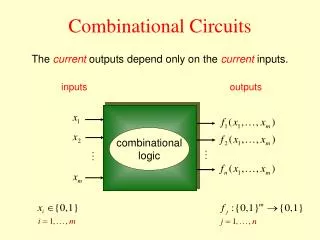
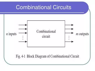
COMBINATIONAL CIRCUITS. 1. Combinational 2. Sequential. LOGIC CIRCUITS:. Combinational logic circuits (circuits without a memory): Combinational switching networks whose outputs depend only on the current inputs. Sequential logic circuits (circuits with memory):

E N D
COMBINATIONAL CIRCUITS 1. Combinational 2. Sequential LOGIC CIRCUITS: Combinational logic circuits (circuits without a memory): Combinational switching networks whose outputs depend only on the current inputs. Sequential logic circuits (circuits with memory): In this kind of network, the outputs depend on the current inputs and the previous inputs. These networks employ storage elements and logic gates. [Chapters 5 and 9]
COMBINATIONAL CIRCUITS • Most important standard combinational circuits are: • Adders • Subtractors • Comparators • Decoders • Encoders • Multiplexers Available in IC’s as MSI and used as standard cells in complex VLSI (ASIC)
Designing a Combinational Circuit • From the Specification of the circuit, determine the number of inputs and output. Assign a symbol to each • Derive the Truth Table that defines required relationship between inputs and outputs • Obtain Boolean function for each output as a function of the input variable • Draw the logic diagram and verify the correctness of the design
DESIGNE CRITERIA • MIN NO OF GATES • MIN NO OF INPUTS • MIN PROPAGATION TIME • LIMITATION OF DRIVING CAPABILITIES OF EACH GATE
ARITHMATIC OPERATIONS • BASIC OPERATION IS ADDITION OF TWO BINARY DIGITS. WHEN 0+0=0, 0+1=1, 1+0=1. AND 1+1=10. • THEN FIRST THREE OPERATIONS PRODUCE SUM OF ONE DIGIT • FORTH PRODUCE TWO DIGITS. HIGHER SIGNIFICANT BIT IS CALLED A • CARRY
Binary Adder-Subtractor • Most Basic arithmetic function is Addition of two binary digits • 0+0=0, 1+0=1, 0+1=1, 1+1=10 (Carry) • Carry is added to the next higher order pair of significant values • A combinational circuit that performs addition of two bit is called Half Adder • A combinational circuit that performs addition of three bits is called Full Adder (Adding two half adder) • Binary Adder Subtractor performs addition and subtraction
X Y S C 0 0 0 0 0 1 1 0 1 0 1 0 1 1 0 1 BINARY ADDER – Half Adder
Inputs Outputs x y z S C 0 0 0 0 0 0 0 1 1 0 0 1 0 1 0 0 1 1 0 1 1 0 0 1 0 1 0 1 0 1 1 1 0 0 1 1 1 1 1 1 BINARY ADDER - Full Adder INPUTS OUTPUTS C
X Y D B 0 0 0 0 0 1 1 1 1 0 1 0 1 1 0 0 TRUTH TABLE H/SUB
Inputs Outputs x y z B D 0 0 0 0 0 0 0 1 1 1 0 1 0 1 1 0 1 1 1 0 1 0 0 0 1 1 0 1 0 0 1 1 0 0 0 1 1 1 1 1 TRUTH TABLE F/SUB
CODE CONVERTIONBCD TO EXCESS-3 • INPUTOUTPUT EX-3 A B C D W X Y Z 0 0 0 0 0+3 0 0 1 1 0 0 0 1 1+3 0 1 0 0 0 0 1 0 2+3 0 1 0 1 0 0 1 1 3+3 0 1 1 0 0 1 0 0 4+3 0 1 1 1 0 1 0 1 5+3 1 0 0 0 0 1 1 0 6+3 1 0 0 1 0 1 1 1 7+3 1 0 1 0 1 0 0 0 8+3 1 0 1 1 1 0 0 1 9+3 1 1 0 0 DRAW K-MAPS WITH Don,t Care for WXYZ. DRAW DIAGRAM
Analysis Procedure • Determine the function that circuit implements • Ensure that circuit is combinational and not sequential • No feedback (Output of one circuit as a input to another) • Logic diagram • Obtain the Boolean function or truth table
Inputs Outputs A B C F1 F2 0 0 0 0 0 0 0 1 1 0 0 1 0 1 0 0 1 1 0 1 1 0 0 1 0 1 0 1 0 1 1 1 0 0 1 1 1 1 1 1 ANALYSIS OF COMBINATIONAL LOGIC INPUTS OUTPUTS From the truth table can you tell the function of the circuit?
MULTI LEVEL NAND CCTS REPLACE INVERTERS WITH NAND GATES FUNCTIONS REMAIN THE SAME
MULTI LEVEL NAND CCTS • BOOLEAN FUNCTION IMPLEMENTATION • F= A(B+CD)+BC’ • STEP -1. From Algebric Expression draw Logic Diagram with AND ,OR. NOT Gates. • STEP -2. Draw 2nd Logic Diagram with NAND Gates. • STEP 3. Remove Casecade Inverters.Remove Single Inverter and complement Variable. • F= (A+B’)(CD+E)
ANALYSIS PROCEDURE • STEP-1. Given Logic Diagram. • STEP-2 Boolean Function. • STEP-3 Truth Table. • STEP-4 K-Map • STEP-5 Function
BLOCK DIAGRAM TRANSFORMATION STEP-1 Draw NAND Logic Diagram Remove Bubbles Step-3 COVERT NAND TO AND INVERT and INVERT OR STEP-2
MULTI LEVEL NOR CIRCUITS REPLACE NOT WITH NOR GATES ANALYSIS PROCEDURE AND BLOCK DIAGRAM TRANSFORMATION IS THE SAME AS NAND CCTS
X OR COVERED IN CHAP 3 EXCLUSIVE-OR AND EQUIVALENCE FUNCTIONS ALREADY COVERED IN 3RD CHAPTER
BCD Excess 3 Code • Digit 8 • Company • 1 Manager • 2 Clerk • 1 Guards • During office hours When manager present atleast one clerk • During office hours When Manager missing both clerks should be present • After Business hours guard should be present • Input • Manager A, Clerk B, Clerk C, Guard D, Businesshours E • Output • Alarm F
DESIGN OF COMBINATIONAL LOGIC Example: Design a combinational circuit with three inputs and one output. The output is a 1 when the binary value is less than three. The output is 0 otherwise. y y z 00 01 11 10 0 x 1 z
Binary Adder • Binary Adder is a circuit that produces sum of two binary number • It can be constructed with full adders (FA) connected in cascade, with output carry from one connected to the input carry of the next full adder • For Example 1011+00111110 3 2 1 0 i
CASCADE 4-BIT FULL ADDER BINARY ADDER 3 2 1 0 i • For Example • 1011+001111110
Carry Propagation Addition of two numbers in parallel implies that all bits are available for computation. Total propagation delay = propagation delay of a gate # gate levels In this case no of gate levels are =8 available only after C3 has propagated through
Carry Propagation Q: Find the total C propagation delay in the 4-bit full adder circuit. Although some out (1/0) will be there, it may not be correct. Stable value only after carry propagation
Carry Propagation The carry propagation time is a limiting factor on the speed with which two numbers are added. The most widely technique for reducing the carry propagation time in a parallel adder uses the principle of carry lookahead If define two variables P & G. Carry Propagate from Ci to Ci+1 Carry Generate from Input
Carry Lookahead Generator Boolean Function for Carry is expressed in SOP (2 level AND and OR gate)
4-bit Adder with Carry Lookahead XOR Generates P AND Generates G
Overflow Overflow occurs when two numbers of n digits are added and the sum occupies n +1 digits. If V = 0 no overflow: n-bit results is correct. If V = 1 overflow: The result contains n + 1 bits, and the (n+1)th bit is the actual sign.( It means for 8bits we need 9bits)
Decimal Adder BCD Adder • Binary adder (1+1) Bit + 1 Carry= 3 bits • BCD(4+4) Bits + 1 Carry= 9 bits input • Max output is 9+9+1=19 • 4 bit adder • Input 2 BCD numbers • Sum will be in binary form • Output binary number from 0 to 19 • AIM: Convert Binary back to BCD • When Binary Sum >1001 Add 0110 to corresponding Binary number for correction. • Correction is needed when K=1 • For no 1010 to1111 need correction, have 1 in Z8 and Z4 or Z8 and Z2 Thus Boolean Function C=K+Z8Z4+Z8Z2. will be used to get C=1 It will apply 0110 to second 4bit Adder and carry in the output. • Second addition take place. If carry occurs neglect it.
Magnitude Comparator A magnitude comparator is a combinational circuit that compares two numbers, A and B, and then determines their relative magnitudes. A > B A = B A < B NOT REQUIRED BUT CAN BE EXPLANED IF STUDENT WISH Consider two numbers, A and B, with four digits each: Algorithm XNOR (note mistake p. 133) For equality to exist, all variables must be equal to 1:
Magnitude Comparator To determine if A is greater than or less than B, we inspect the relative magnitudes of significant digits. If the two digits are equal, we compare the next lower significant pair of digits. The comparison continues until a pair of unequal digits is reached. The sequential comparison can be expressed by: Compare:
DECODERS • A decoder is a combinational circuit that converts binary information • from n input lines to 2n unique output lines. • i.e. Given a binary number input we want a specific output. • Applications: • Microprocessor memory system: selecting different banks of memory. • Microprocessor I/O: Selecting different devices. • Microprocessor instruction decoding: Enabling different functional • units. • Memory: Decoding memory addresses (e.g. in ROM). • Bell for Mess Kitchen
3-to-8-line DECODER Truth Table • Three inputs are decoded into eight outputs, each representing one of the minterms of the three input variable • If the input corresponds to minterm mi then the decoder ouputi will be the single asserted output. • Binary to OCTAL conversion IS ONE OF ITS APPLICATION
2-to-4-line DECODER with Enable Input The decoder is enabled when E = 0. The output whose value = 0 represents the minterm is selected by inputs A and B. The decoder is disabled when E = 1 D0 … D3 = 1 A Decoder with enable input is called a decoder/demultiplexer. Demultiplexer receives information from a single line and directs it to the output lines. Multiplexer is opposite of DeMultiplexer (Concept can be used to share Network) Complemented outputs