Download
1 / 3
30 likes | 175 Vues
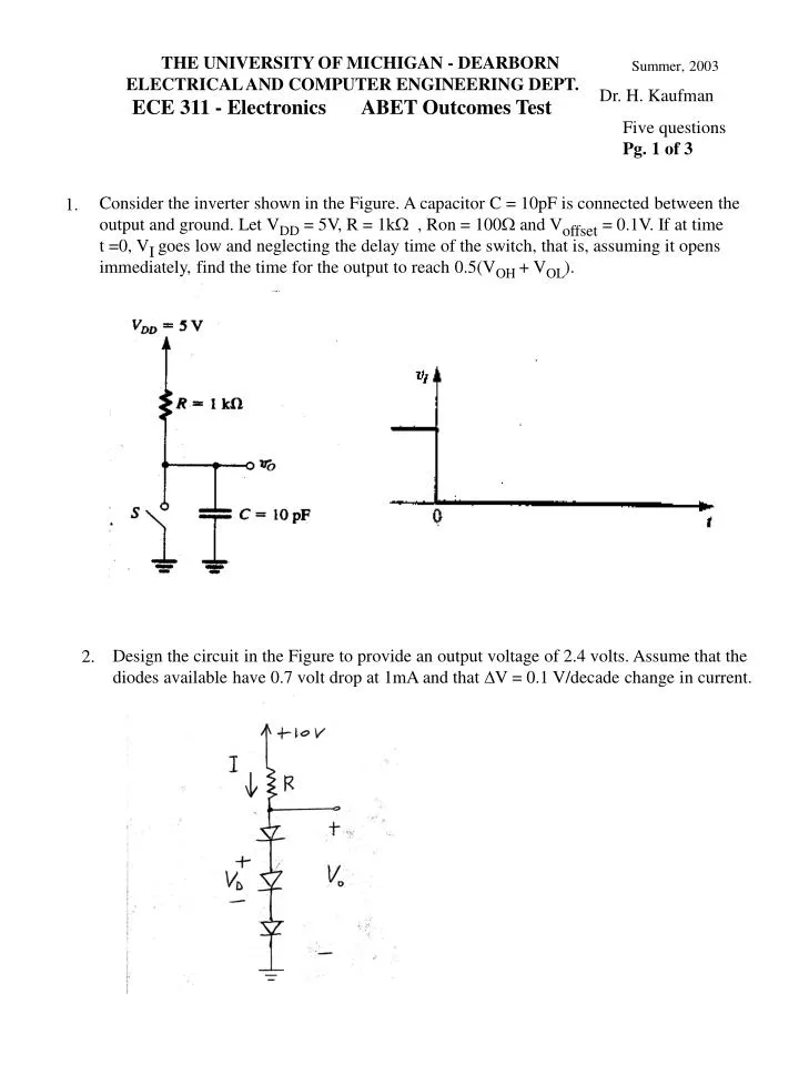
THE UNIVERSITY OF MICHIGAN - DEARBORN ELECTRICAL AND COMPUTER ENGINEERING DEPT. ECE 311 - Electronics ABET Outcomes Test. Summer, 2003. Dr. H. Kaufman. Five questions Pg. 1 of 3. Consider the inverter shown in the Figure. A capacitor C = 10pF is connected between the

E N D
THE UNIVERSITY OF MICHIGAN - DEARBORN ELECTRICAL AND COMPUTER ENGINEERING DEPT. ECE 311 - Electronics ABET Outcomes Test Summer, 2003 Dr. H. Kaufman Five questions Pg. 1 of 3 Consider the inverter shown in the Figure. A capacitor C = 10pF is connected between the output and ground. Let VDD = 5V, R = 1kW , Ron = 100W and Voffset = 0.1V. If at time t =0, VI goes low and neglecting the delay time of the switch, that is, assuming it opens immediately, find the time for the output to reach 0.5(VOH + VOL). 1. Design the circuit in the Figure to provide an output voltage of 2.4 volts. Assume that the diodes available have 0.7 volt drop at 1mA and that DV = 0.1 V/decade change in current. 2.
ECE 311 ABET Outcomes Test Summer 2003 pg. 2 of 3 3. For the common-emitter amplifier shown in the Figure, let VCC = 9V, R1 = 27kW , R2 = 15kW , RE = 1.2kW , and RC = 2.2 kW . The transistor hasb = 100. (a) Calculate the DC bias current IE. (b) Draw the SSAC model for the transistor circuit and calculate any required AC parameters. (c) What is the voltage gain vo/vs (d) What is the input impedance (e) What is the output impedance. (a) Draw the CMOS inverter. (b) What is the required relationship between (W/L)p and (W/L)n for which the transistors Qn and Qp are said to be matched and the CMOS inverter is made to switch at the midpoint of logic swing, (i.e. at VDD/2 ) ? 4. 5. Draw the transfer characteristic for the Class B output stage and circle the region in which “crossover distortion” occurs. Assume that Qn and Qp have collector-emitter saturation values VCENsat and VECPsat respectively.
ECE 311 ABET Outcomes Test Summer 2003 pg. 3 of 3 The circuit shown in the Figure is intended to supply current to floating loads (those for which both terminals are ungrounded) while making the greatest possible use of the available power supply. (a) Assuming ideal op amps, sketch the voltage waveforms at nodes B and C for a 1-V peak –to-peak sine wave applied at A. Also sketch vO. (b) Assuming that the op amps operate from + 15V power supplies and their output saturates at + 14 V, what is the largest sine wave output (peak to peak value) that can be accommodated? 6. - + - + (c) Give at least four characteristics of an ideal op-amp (Hint: what is open loop gain, output resistance, bandwidth, current into each input? (d) What is meant by the term “slew rate”?